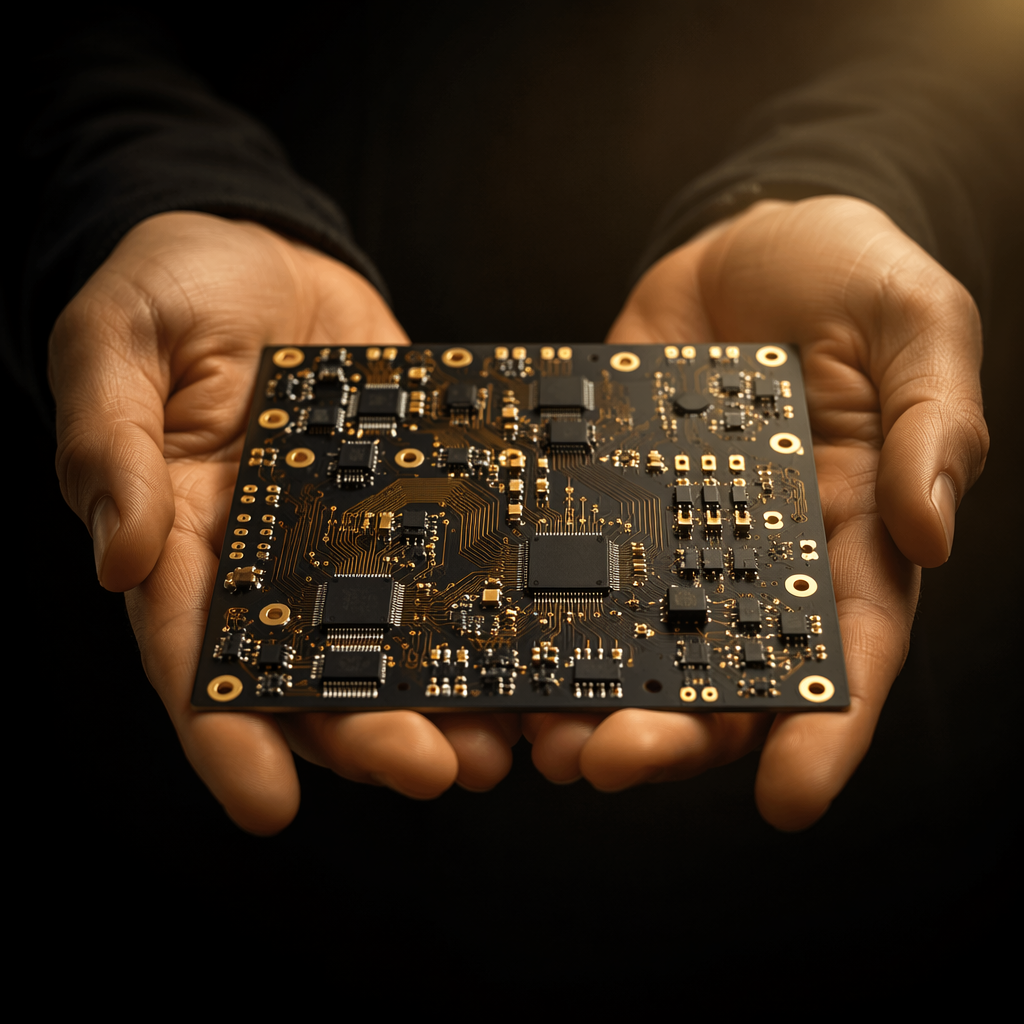
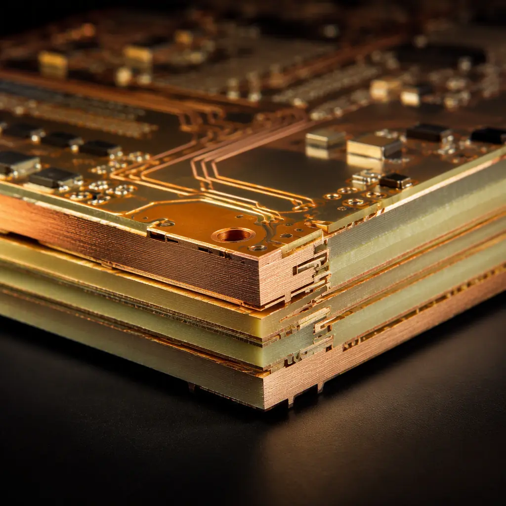
A laminate has two numbers that decide whether an RF board works: the dielectric constant (Dk) and the dissipation factor (Df). Dk controls how the signal wavelength maps to copper geometry, and Df controls how much energy the material itself loses. FR-4 has a Dk of about 4.2 and a Df of 0.018; a high-speed Rogers laminate such as the 4000-series sits around 3.5–3.6 Dk with a Df as low as 0.002. That roughly order-of-magnitude gap in loss is exactly why you reserve the premium material for the regions that need it. At Huaxing PCBA we build 32-layer boards and support a range of substrates from FR-4 to Rogers, PTFE and ceramic, so hybrid constructions are a routine part of our RF work. See our PCB materials guide for the material family overview.
The catch is that hybrid is not a single material. It is two (or more) laminates and their prepregs laminated into one board, and that joining process is where dimensional mismatch, delamination and impedance drift come from. A hybrid stackup must match the coefficient of thermal expansion (CTE) of the layers, choose the right bonding prepreg, and give the impedance a controlled second conductor no matter which region a trace sits in. We build IATF 16949 and ISO 9001 certified boards and run ±5% impedance control with TDR verification, which is the tool you use to head off hybrid problems.
When a Hybrid Stackup Is Actually Worth It
The reason to hybridise is simple: a full low-loss laminate board can be three to five times the material cost of the same board in FR-4. But that cost is only justified where the signal demands it. A mixed-signal board with a 5 GHz radio on one corner and a 10 MHz Ethernet controller on the other is the classic case — one region needs low Df and controlled Dk, the other is happy on FR-4. Putting the expensive laminate only under the RF traces is the efficient call.
| Region | Needs | Material choice |
|---|---|---|
| RF front end, antenna, filter | Low Df, stable Dk, tight tolerance | Rogers 4003C / 4350B, low-loss PTFE |
| High-speed digital (SerDes, DDR) | Moderate loss, controlled impedance | Low-loss FR-4 or hybrid region |
| Power plane / control / interface | Cheap, robust, high Tg | FR-4 (Tg 170 or higher) |
| Antenna ground / low-signal | Cost, stack-up rigidity | FR-4 |
The decision should be driven by measured requirements, not habit. If your transceiver needs a Df below about 0.005, a standard FR-4 will not do the job and a low-loss laminate (or a hybrid with it) is justified. Above that, the cost of premium material buys very little. Before you commit, read our RF PCB design guide and our PTFE high-frequency guide to see how far the materials scale.
The Two Numbers That Split the Board: Dk and Df
Hybrid construction makes the dielectric non-uniform, and that has a direct effect on your impedance and your wavelength. When a trace crosses from a region with one Dk to another, the controlled-impedance depth changes and the trace either becomes too wide or too narrow to hit its target. So the transition region is the design problem.
Keep each trace within a single Dk field
Do not route a 100Ω differential pair so that half of it is over the RF laminate and half over FR-4. The impedance will be different in each half and you will get a reflection at the boundary. Keep a controlled-impedance trace fully within one material region, and put the impedance transition at a soldered component where the field is interrupted anyway.
Design the transition as a deliberate junction
When a signal genuinely moves from the RF region to the digital region, put a pad or a matching network at the boundary so the change in Dk is absorbed where you can compensate, rather than as a hard step in a bare trace. This is where the impedance control discipline pays off.
Verify with TDR, not just a field solver
A field solver tells you what the stackup should be; a TDR on the production board tells you what it actually is. Hybrid boards drift at the material boundary, so TDR verification of the targeted traces is the check that catches a real problem. We run TDR as standard on controlled-impedance boards.
CTE Matching: Why Mixed Laminates Delaminate
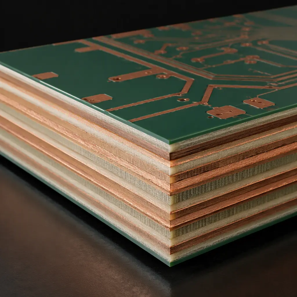
FR-4 expands roughly 12–16 ppm/°C in-plane, while a Rogers laminates and copper move at ~17–20 ppm/°C (and low-XY PTFE moves differently again). When you bond two materials with different in-plane CTE, thermal cycling creates shear stress at the interface. Over hundreds of cycles, that stress can crack the plated barrels or start a delamination at the polymer bond, which is exactly why you choose a bonding layer that accommodates the mismatch and why reliability testing on a hybrid product is non-negotiable.
Key Takeaway: It is not the RF laminate that is fragile — it is the joint between the two laminates. Choose a low-flow or no-flow prepreg with a CTE that bridges the two materials, and validate the hybrid with thermal cycling and solder reflow simulation before you commit to volume. This is a fabrication knowledge problem, not a schematic one.
| Material | Typical Dk | Typical Df | In-plane CTE (ppm/°C) |
|---|---|---|---|
| Standard FR-4 | 4.2 | 0.018 | ~12–16 |
| High-Tg FR-4 | 4.2–4.4 | 0.016 | ~14 |
| Rogers RO4003C | 3.55 | 0.0027 | ~11–14 |
| Rogers RO4350B | 3.66 | 0.0037 | ~11–14 |
| PTFE (low loss) | 2.2–2.9 | 0.0009–0.002 | ~20–30 |
Prepreg Selection for the Bond Layer
The bond between the RF laminate and the FR-4 is made by a prepreg, and the choice determines both the reliability and the impedance of any trace passing through or near it. In a hybrid, the prepreg is often different from the one you would use for a pure FR-4 stackup.
- Low-flow prepreg minimises resin bleed into the RF region, which matters when the RF laminate has a tight Dk tolerance and you do not want resin to line the pad edges.
- No-flow prepreg is used when you are bonding over an inner region where you must avoid resin moving into a cavity or a tight trace.
- Thermally conductive prepreg helps move heat out of the RF power regions, useful when the amplifier section runs hot.
- CTE-bridging prepreg is the pragmatic insurance for a dissimilar-material joint, reducing the shear stress the thermal cycles impose.
The cost interaction here is real: the prepreg and the extra lamination cycles are part of the reason a hybrid board is more expensive than a single-material board even before you count the laminate itself. Our PCB stackup design guide walks through how the prepreg choice cascades into cost and impedance.
Layer Ordering and Where the RF Core Goes
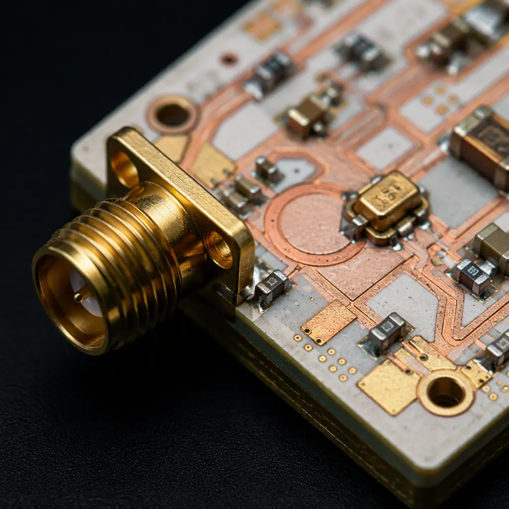
The geometry of the hybrid stackup matters as much as the material. Because RF is predominantly a surface or near-surface phenomenon for many designs, the RF laminate is usually placed just under the top copper, with FR-4 carrying the bulk of the core and the bottom. That gives the RF traces a short, well-controlled return and keeps the expensive material thin.
For a mixed-signal board with a high-speed SerDes on the same board, the two premium regions may be separate — one for RF, one for the high-speed traces — and the stackup should be built so each has its own controlled impedance channel rather than sharing one. A mmWave or antenna design may go further and use a thin, low-loss core just for the top layer. The tradeoff is that the number of real laminates in a hybrid tends to go up, which raises the layer count and the cost. That is the point where you talk to the fab about what is actually manufacturable, not just what the field solver likes.
Manufacturing Notes That Keep a Hybrid Board Reliable
Control the drilling and registration
Hybrid boards have layers of different stiffness, and the drill can wander or the hole-accuracy can slip. A stable lamination plan and tight tooling registration keep the vias aligned. Ask your fab for the drill registration tolerance up front.
Bake and control moisture before reflow
Low-loss laminates are less porous than FR-4 but the joint can still absorb and then violently outgas moisture during lead-free reflow. A proper bake and moisture control, per our moisture sensitivity guide, is the cheap insurance against popcorning.
Validate with cross-section and thermal cycling
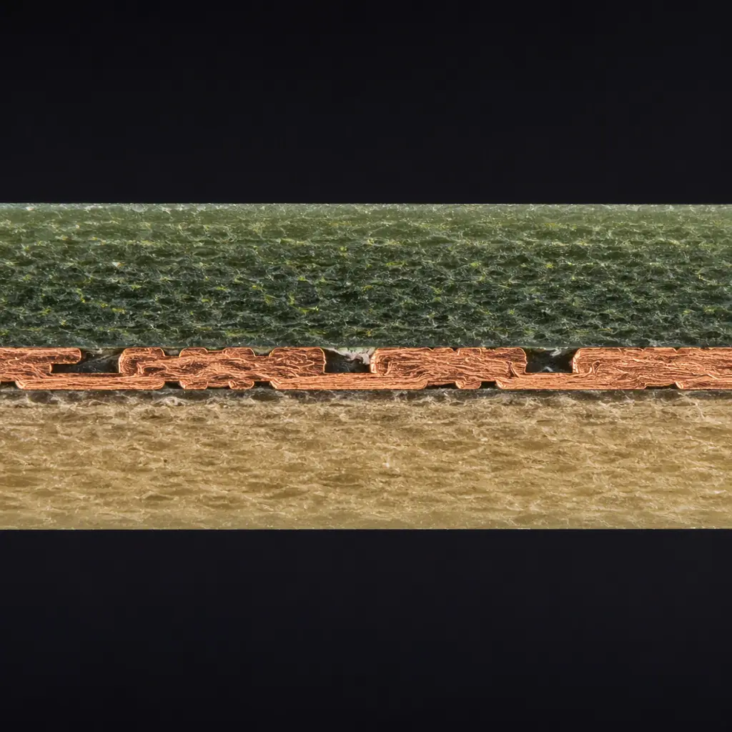
A cross-section at the hybrid joint tells you whether the bond is void-free and whether the plated barrel is healthy after reflow. Thermal cycling and reflow simulation on a pre-production sample is what proves the CTE story in practice. We offer both as part of a qualification program.
Summary: Hybrid Is a Fabrication Decision as Much as a Design One
A hybrid Rogers + FR-4 stackup is the smart way to get RF-grade performance at a controlled cost, but it moves the engineering from the schematic to the material and the lamination. Match the Dk and Df to the region, keep each trace in one Dk field, bridge the CTE with the right prepreg, order the layers for a clean return, and validate with TDR, cross-section and thermal cycling. Done well, the board is cheaper and just as reliable as a full low-loss board.
At Huaxing PCBA we build IATF 16949 and ISO 9001 certified boards up to 32 layers and 3/3 mil line and space, with ±5% impedance control, TDR verification, 0.3 mm pitch and 0201 placement, and X-ray and AOI inspection. We have built hybrid, mixed-material RF boards for RF, 5G, radar and GNSS programs. Get a quote or talk to our engineering team about your mixed-signal stackup and we will tell you the manufacturable, costed answer.