

Silkscreen, also called the legend, is the white layer of text and symbols screened onto the board surface to identify components, show orientation and mark version and polarity. It does not carry current, so it is easy to treat as a cosmetic afterthought — but the legend is read by the stencil printer, the pick-and-place operator, the rework technician and often an end customer. A design with 0.10 mm trace widths can be a production winner, yet fail on the bench because a 0.6 mm reference designator is indistinguishable from the pad it points to. At Huaxing PCBA we build IATF 16949 and ISO 9001 certified boards on 8 SMT lines with 8M placements/day, and we run a DFM review on every incoming legend. See our Gerber files and DFM guides for the wider handoff.
This guide covers the rules that actually matter: minimum line width and character height, clearance to copper and pads, where reference designators belong, how to mark polarity and pin-1, and the checks our engineers run so your legend is readable after assembly — not just in the CAD file.

What the Silkscreen Layer Does — And What It Cannot Do
Silkscreen identifies components and gives assembly cues, but it is strictly non-conductive and is not a substitute for a copper feature. It cannot carry a reference, a test point, or a soldering pad. The legend is screened onto the top of the solder mask in most fab runs, which means the legibility of a character is bounded by the contrast between the ink and the underlying mask — not by anything you can size up in the board editor.
The practical consequence: legend text that is technically within the fab minimum may still be unreadable in production because the mask underneath is the same colour family. The standard advice is to keep legend clear of pads and exposed copper, because ink over a pad lifts during soldering and ink over copper can read as an extra feature to an automated optical inspection (AOI) system.
| Legend element | Function | Main risk if wrong |
|---|---|---|
| Reference designators (R1, C2, U3) | Identify each part for assembly, rework and BOM cross-check | Operator misloads a resistor; rework probes the wrong component |
| Component outlines and values | Show footprint orientation and part value at a glance | Wrong polarity install; incorrect value assembled |
| Polarity, pin-1, notch and dot marks | Prevent reversed capacitors, diodes and ICs | Catastrophic reverse assembly — the most expensive legend failure |
| Version, date and ECN text | Identify which board revision is on the bench | Wrong revision tested against the wrong documentation |
IPC-2221 Silkscreen Readability Rules: The Numbers to Design To
IPC-2221 (and the universal-design guidance it pulls from) sets baseline dimensions for a legend that will survive fabrication and remain readable at assembly. These are not suggestions — they are the thresholds most fabricators use for their own min-line and min-space checks.
Minimum line width — 0.15 mm (6 mil)
Below about 0.15 mm the ink tends to bridge or break during screening. If you need finer detail, move it to the copper layer and photo-etch it (see solder mask and layer selection).
Recommended character height — 1.0 mm (40 mil), minimum 0.8 mm
Most fabricators treat 1.0 mm as the comfortable default for reference designators. At 0.8 mm the text is still printable but starts to coalesce after solder mask, so treat that as an absolute floor rather than a target.
Clearance to copper and pads
Keep a minimum of 0.1 mm between legend and exposed pads, and 0.15 mm to copper features. Legend over an exposed pad lifts off during wave or hand-soldering and can leave the pad looking shorted to an AOI camera.
These dimensions are the reason a dense fine-pitch board often ends up with very little silkscreen: the space simply is not there at 0.15 mm stroke width. On such boards, the practical answer is to shrink the legend to bare essentials (pin-1, polarity, reference designators at component edges) and move the rest to the copper or documentation layer.
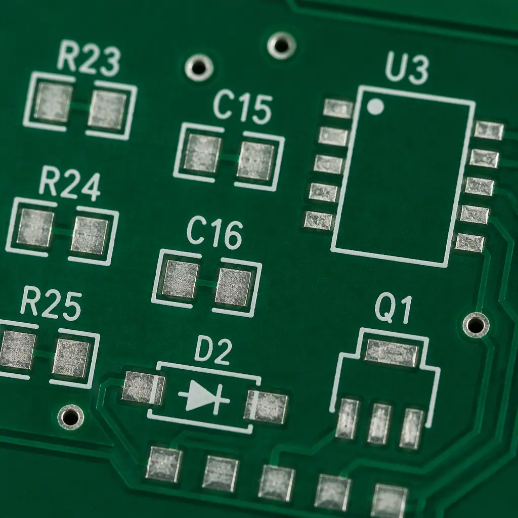
Reference Designator Placement: Put It Where a Person Can Read It
The rule is simple: the designator must be visible and unambiguous after the component is placed. That means it goes beside or above the footprint, not underneath it, and it reads in a consistent orientation so the operator can sweep across the board without rotating the panel.
- Keep one orientation. Rotate all designators to a single reading direction (usually horizontal, bottom-to-top on vertical placement) to avoid the operator flipping the board mid-pass.
- Offset, not centered. Place the designator at the footprint edge so a populated SMT resistor does not hide it. A centered designator disappears the moment the part lands.
- Group connector pin calls. For connectors and ICs, put the pin-1 or pin-A mark at the correct end and label the pin fields so the cable or daughter card mates correctly. See our design-for-testability guide.
- Fit the value, not just the ref. If a 0603 resistor is too small for its value text, let the ref designator carry the identification and put the value on the BOM where it belongs.
Polarity, Pin-1 and Orientation Marks: The Cheap Insurance
The most expensive silkscreen failures are not illegibility — they are reversed components. A capacitor soldered backwards can pop, an LED reversed will not light, and an IC rotated 180° can let the magic smoke out. All of these are preventable with a legend that unambiguously marks the correct orientation.
| Component | Mark that prevents reversal | Where it goes |
|---|---|---|
| Polarized electrolytic / tantalum | Plus (+) sign | At the positive end, next to the pad |
| Diode | Band / bar at cathode, arrow at anode | At the cathode end |
| IC / QFN / BGA | Dot, notch or pin-1 chamfer | At pin 1 |
| SMD LED | Anode arrow and cathode flat | At the correct end, clearly |
| Connector | Pin-1 or pin-A label | At the mating reference |
On a mixed circuit with high-side and low-side components, a second, subtler orientation trap appears: a reference designator that looks the same upside-down. If your audience may read the board from either side, add a visible board-orientation arrow (often the "this way up" mark near the connector) so no one has to guess.
Key Takeaway: Orient all polarity and pin-1 marks consistently and place them adjacent to the pad they belong to, not across the component. In our experience the rework rate is the single best metric for whether your legend is doing its job — and the vast majority of misload errors trace back to a missing or ambiguous pin-1 or polarity mark.
Legend Over the Mask vs Over Copper: Contrast, AOI and Readability
The legend layer is printed either over the bare board or over the solder mask, depending on which is last in your stackup. Legend over bare laminate has the highest contrast but is only possible when the legend is applied before the mask is cured. In most commercial fab runs the legend goes over the mask, which means the ink sits on top of the final green or black surface.
Two consequences to design for. First, black and dark-blue masks need larger text because contrast drops — a character that reads perfectly on a light green mask can vanish on a black one, especially at 0.8 mm. Second, Automated Optical Inspection (AOI) reads the legend as a feature: a stray mark that crosses a pad can be reported as a defect, adding noise to your first-article inspection. Keep the legend clear of pads and you keep AOI clean. Our solder mask types guide covers the mask side of this trade-off.
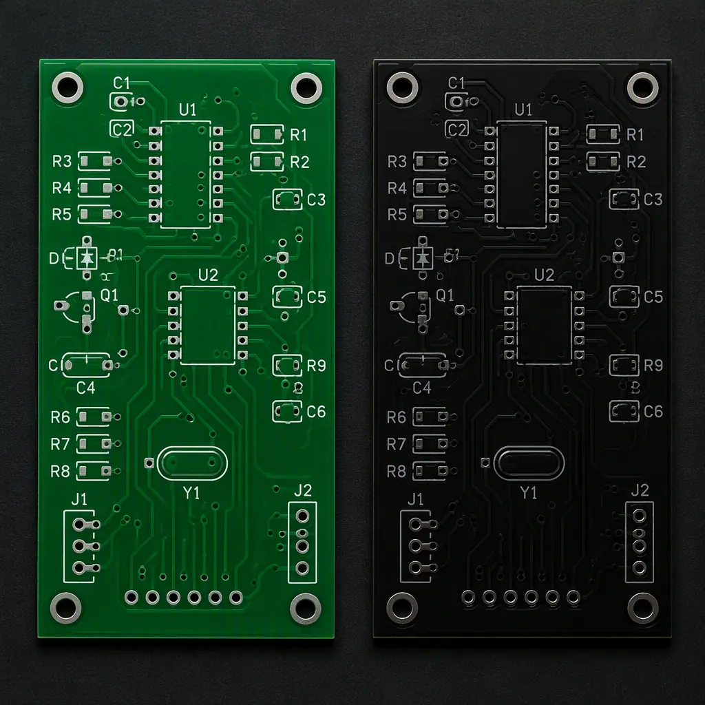
DFM Checks We Run on Your Legend Before Quoting
A legend error is far cheaper to catch in the DFM review than on the assembly line. Before we quote, our engineering team checks the legend against the board data.
Line width and character height floor
Everything below 0.15 mm stroke or 0.8 mm height gets flagged and either enlarged or moved to copper.
Clearance to pads and exposed copper
We check that no legend text or mark overlaps an exposed pad, a test point, or a component footprint that will be populated, because ink there will lift or read as a false defect.
Polarity and pin-1 marks present
Every polarised part and every multi-pin IC should carry an unambiguous orientation mark. If it is missing, we ask before we build — it is cheap to add and costly to discover on a reflowed board.
Value and legend not on the pad side of a two-sided board
Where components sit on both sides, the legend should be split so that each side identifies its own parts. See our stackup guide for layer planning.
Common Legend Mistakes That Cause Scrap or Rework
- Designators under components. The person who needs the reference cannot see it once the part is placed.
- Text smaller than the fab floor. Guarantees broken characters, misreads and rework loops.
- Legend over exposed pads. Ink lifts during soldering and reads as a short to AOI.
- Missing pin-1 / polarity. The single most common cause of a reversed-component failure we see in first articles.
- Chasing fine detail with silkscreen. If you need sub-0.15 mm detail, move it to the copper or documentation layer — ink cannot resolve it.
Summary: Design the Legend for the People Who Read It
Silkscreen is a usability layer, not a decoration. Design to the IPC-2221 defaults — 0.15 mm minimum stroke and 1.0 mm character height — keep legend clear of pads so it prints and inspects cleanly, place reference designators where they are readable after assembly, and make every polarity and pin-1 mark explicit. Do that and your legend will do its real job: preventing the misloads, reversals and rework loops that cost far more than the board itself.
At Huaxing PCBA we build IATF 16949 and ISO 9001 certified boards with heavy copper, metal-core, HDI and up to 32 layers, and we assemble on 8 SMT lines with 8M placements/day, X-ray and AOI inspection. We can review your Gerber data and legend for free, before you commit to a build. Get a quote or ask our engineering team about your silkscreen layer.