

Blog
Technical articles on PCB design, manufacturing, and industry best practices. Written by our engineering team.
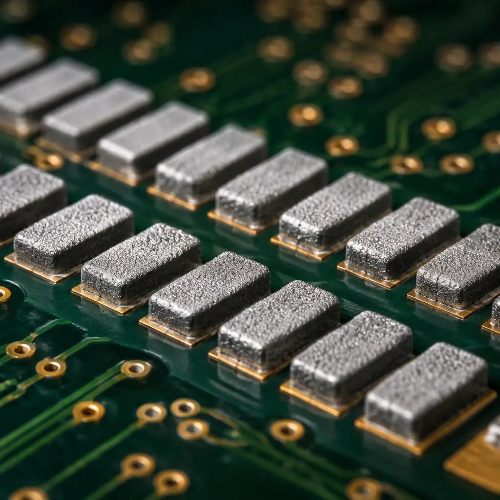
How to use SPI data to control solder paste volume, paste height specs and the process window that keeps a line in control

How to interpret SMT first pass yield correctly: yield definitions that differ between suppliers, benchmark ranges by product class

When nitrogen reflow is worth the cost: O2 ppm targets by component type, the solderability and wetting physics behind it

When stencil-free SMT beats stencils for NPI and prototype builds: tooling cost, changeover time, break-even volume, paste jetting and dispense options

How to evaluate a solder paste jetting machine, and a break-even cost model against stencil printing. For low-volume and high-mix SMT runs

How to calculate SMT line capacity correctly. OEE and bottleneck identification. A planning framework for buyers and manufacturing engineers

PCB silkscreen legend design rules: minimum line width and character height per IPC-2221, reference designator placement, polarity and pin-1 marks
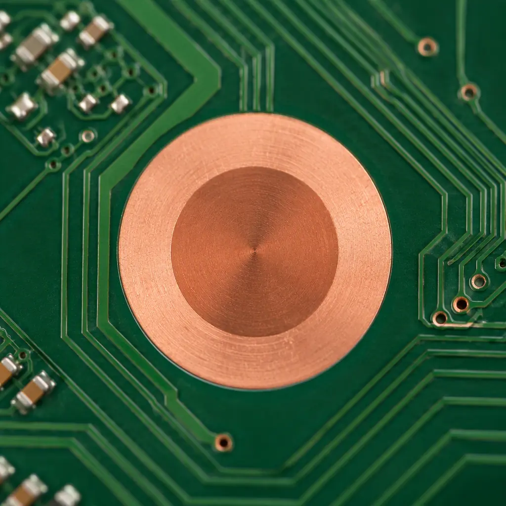
PCB fiducial mark design rules: fiducial size and shape, solder mask clearance, global vs local fiducials, minimum placement from board edge
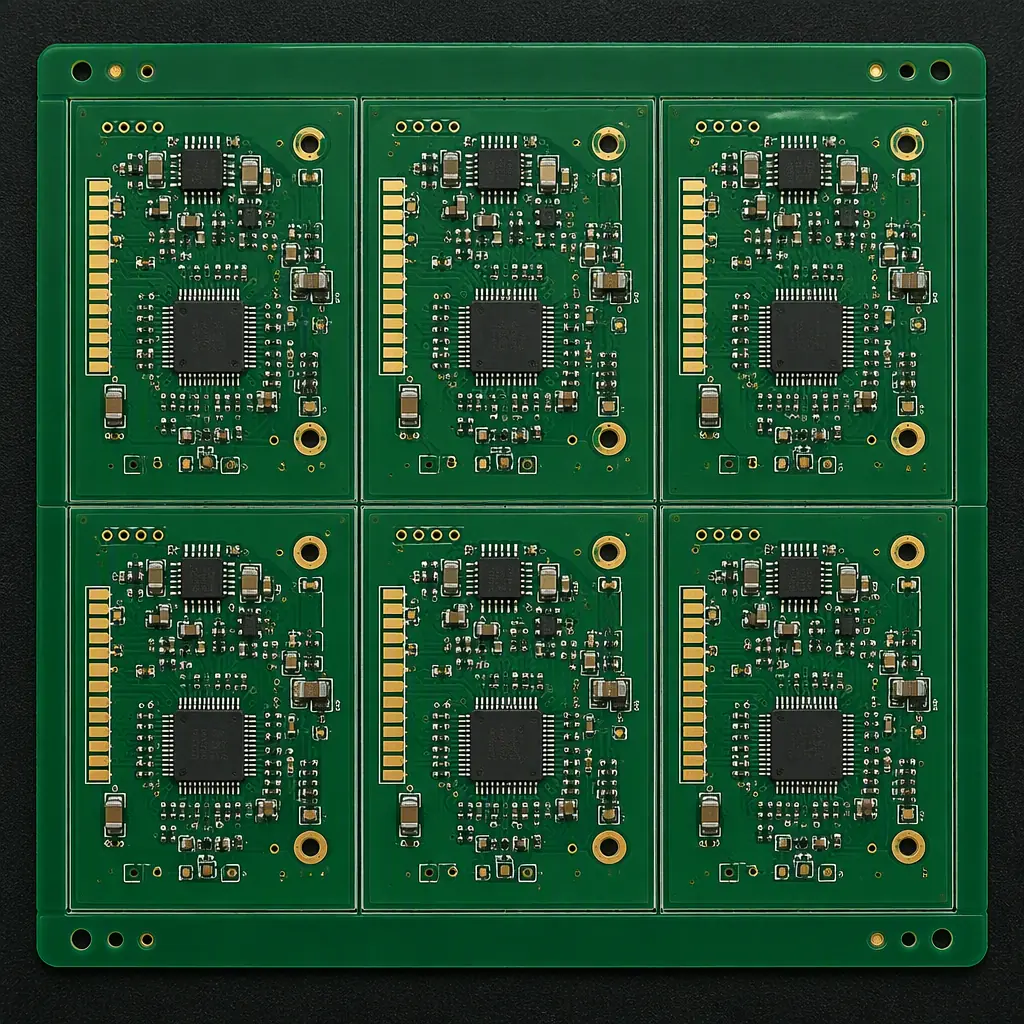
PCB depanelization methods compared: V-score vs tab routing vs laser cutting. Depth rules, edge quality, flexible board handling, cost and yield
Upload your Gerber files and BOM. We'll respond within 24 hours with a detailed quote and free DFM review.