

Blog
Technical articles on PCB design, manufacturing, and industry best practices. Written by our engineering team.
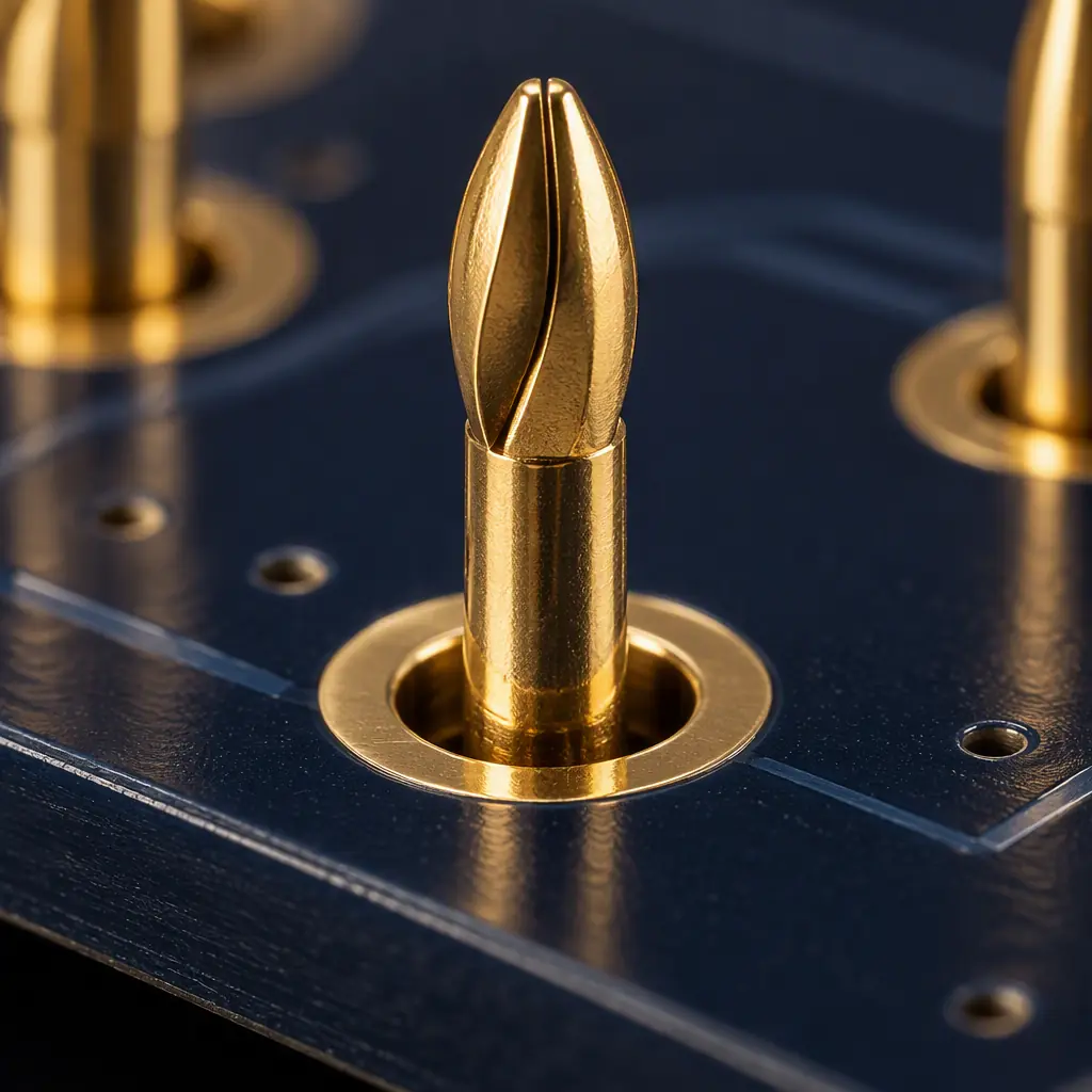
Press-fit connector assembly guide covering finished hole tolerance windows, barrel plating, press-force curve interpretation
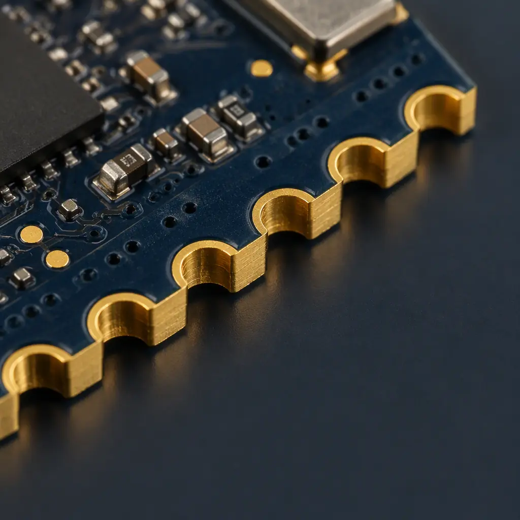
Castellated hole design guide covering half-hole diameter tolerances, barrel plating through the cut, stencil and paste rules, and edge plating
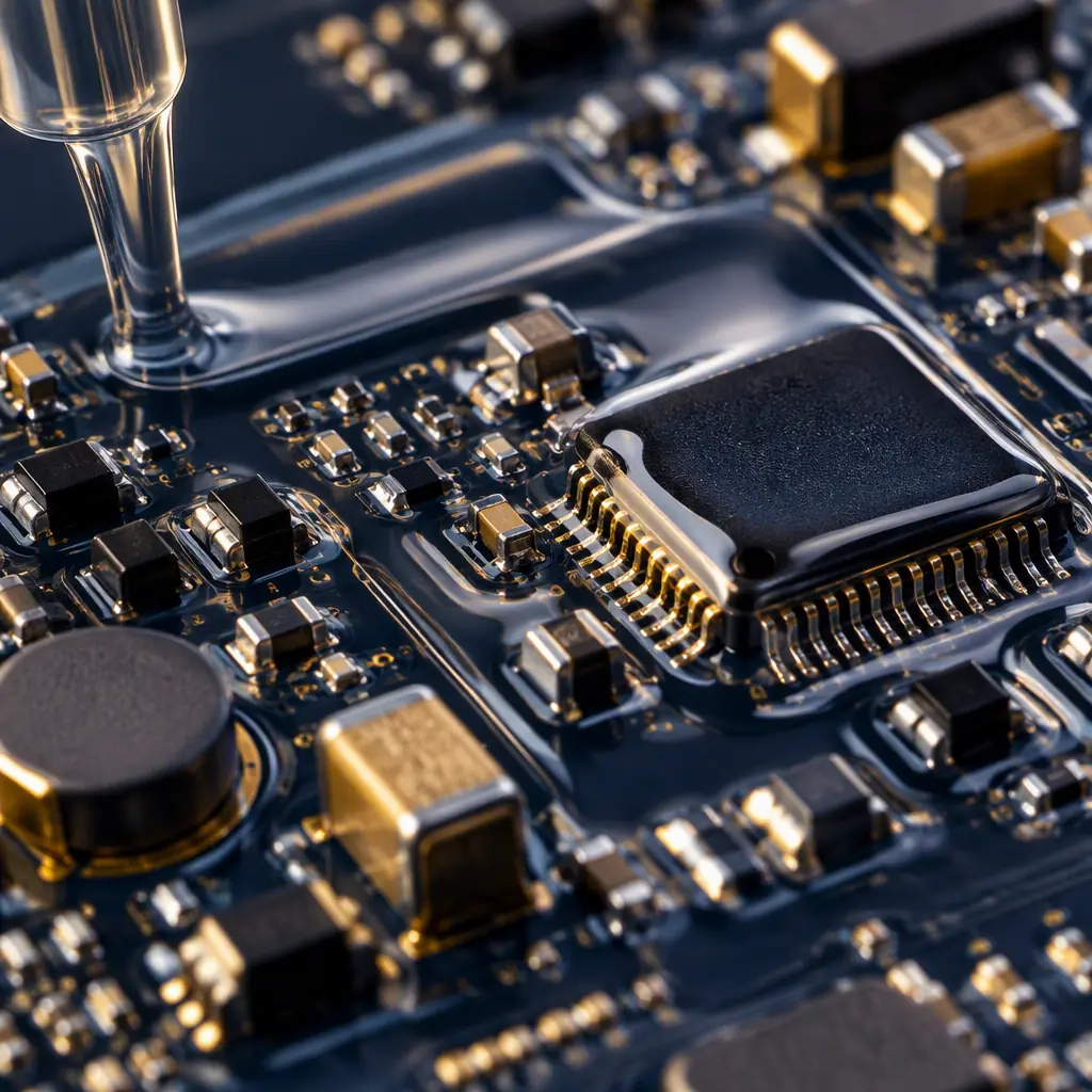
Conformal coating thickness guide covering IPC-CC-830 requirements, wet-film vs cured-film vs microsection measurement
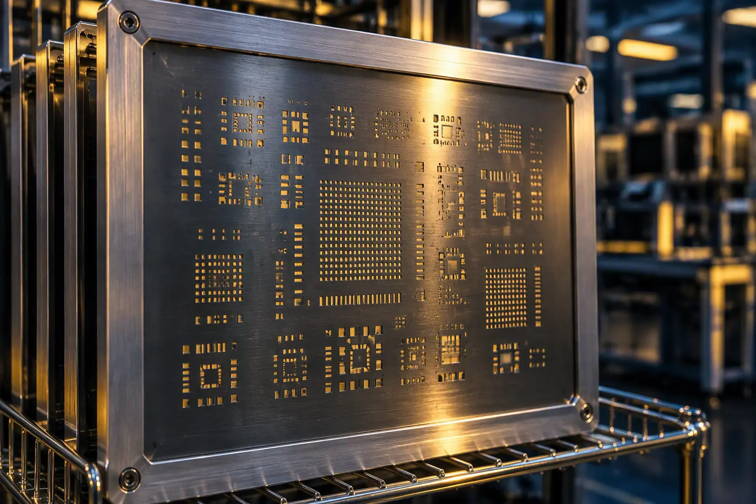
How to manage SMT stencil life by tension measurement, with replacement thresholds and a tool register format

A structured 12-point checklist for visiting a Shenzhen PCB factory: what to inspect, which records to demand and how to convert findings into PO clauses.
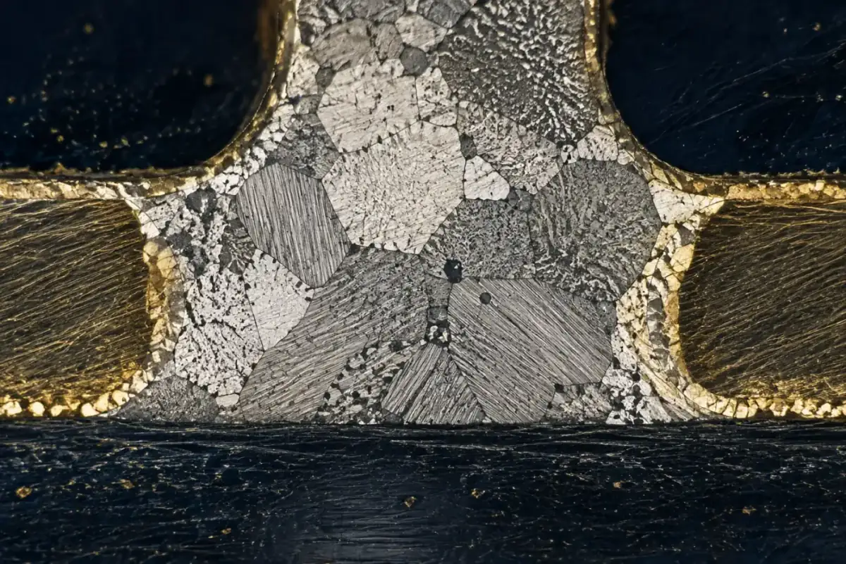
Mixed alloy soldering explained: low-melting phase formation, which SAC305/SnPb combinations are viable, reflow profile rules

What a PCB and PCBA test report package must contain: microsection, impedance, solderability, cleanliness, SPI/AOI/X-ray data, CoC and PPAP documents.
How PCB and PCBA payments are structured by milestone, what qualifies a buyer for net terms and how tooling ownership and deposits work on first orders.
How to specify PCB marking: ink vs laser vs silkscreen, UID and UDI traceability, reflow-rated labels and IPC legibility criteria for buyers.
Upload your Gerber files and BOM. We'll respond within 24 hours with a detailed quote and free DFM review.