

Blog
Technical articles on PCB design, manufacturing, and industry best practices. Written by our engineering team.
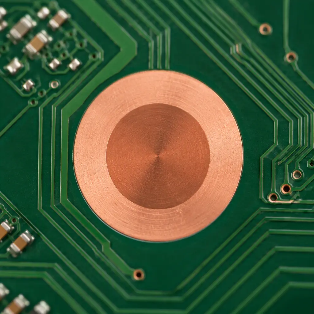
PCB fiducial mark design rules: fiducial size and shape, solder mask clearance, global vs local fiducials, minimum placement from board edge, and how pick-and-p
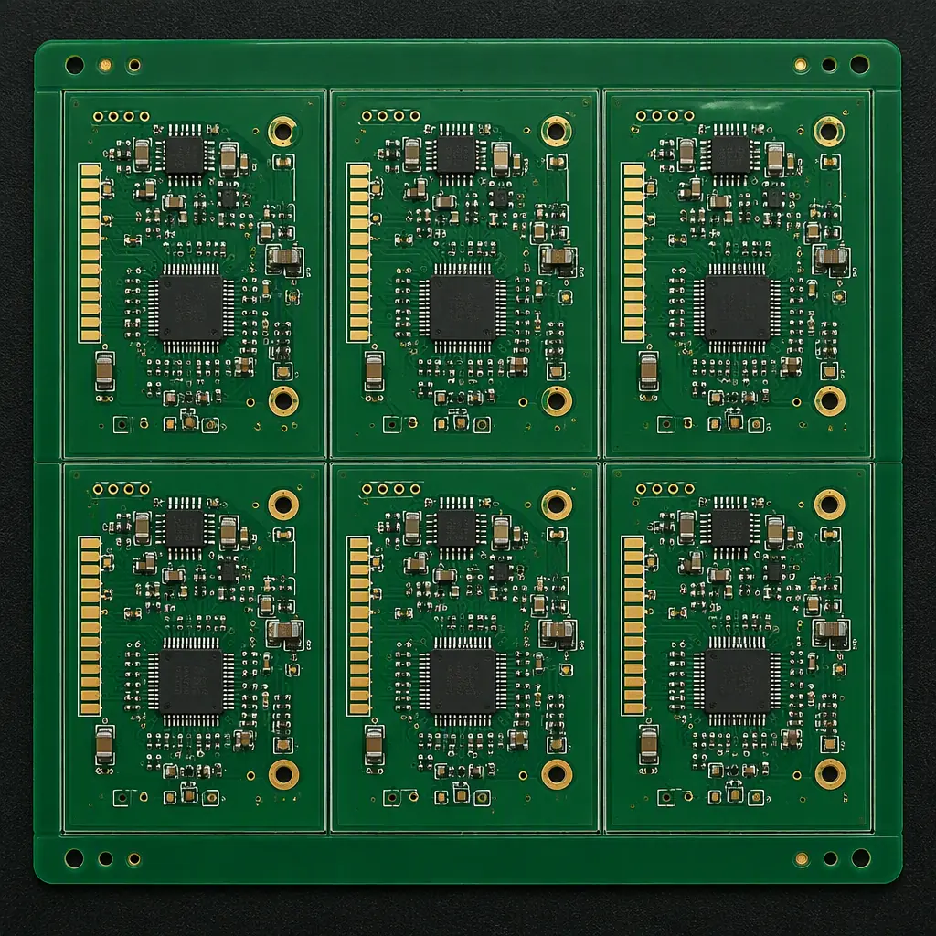
PCB depanelization methods compared: V-score vs tab routing vs laser cutting. Depth rules, edge quality, flexible board handling, cost and yield, and how to cho

PCB silkscreen legend design rules: minimum line width and character height per IPC-2221, reference designator placement, polarity and pin-1 marks, and the DFM
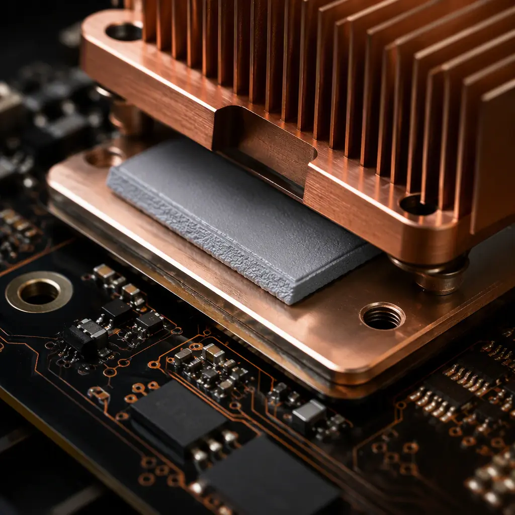
Choose the right thermal interface material (TIM) for a power PCB: gap pad vs thermal paste vs phase-change vs liquid metal, thermal conductivity, thickness, pr
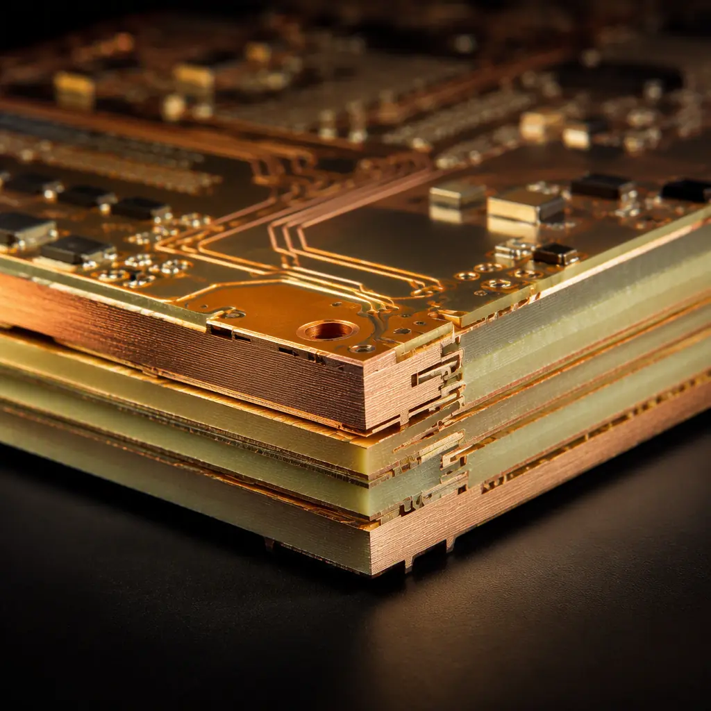
Combine a low-loss RF laminate (Rogers) with economical FR-4 in a single stackup: Dk and Df fields, CTE matching, prepreg selection, layer ordering, impedance p
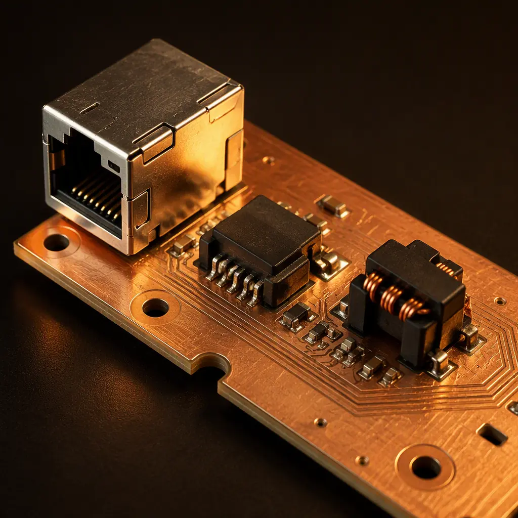
Design the LAN magnetics module right: isolation transformer turns ratio, common-mode choke, 1500V isolation, creepage, Bob Smith termination, and PoE-class mag

CE marking for imported electronic products: which directives apply (LVD, EMC, RED, RoHS), what a Chinese PCBA supplier can actually provide vs what the importe
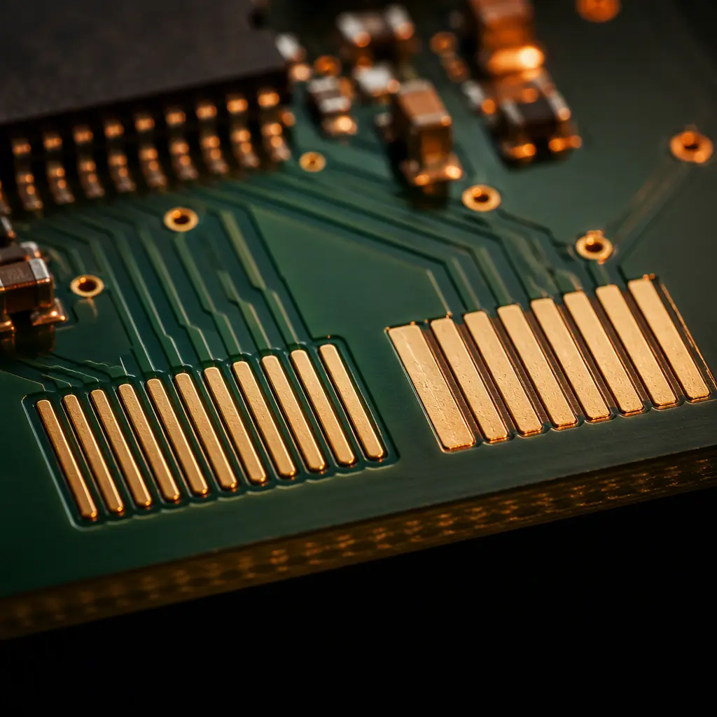
Solder-mask-defined (SMD) vs non-solder-mask-defined (NSMD) PCB pads: how the soldermask opening changes solderable area, fine-pitch wetting, joint strength and

QFN and LGA leadless package soldering: exposed thermal pad voiding, stencil aperture design to IPC-7525, reflow and wetting, and IPC-7093 void acceptance crite
Upload your Gerber files and BOM. We'll respond within 24 hours with a detailed quote and free DFM review.