
Blog
Technical articles on PCB design, manufacturing, and industry best practices. Written by our engineering team.
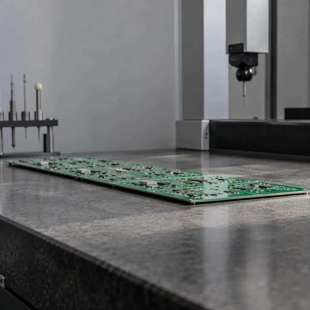
Bow and twist are the two flatness defects that stop a PCB from sitting flat in assembly. The IPC-6012 limits and how to write them into your purchase order
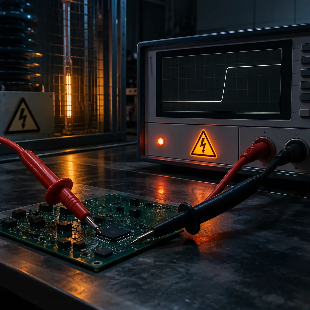
Hi-pot testing proves insulation integrity: not component function. How the withstand voltage is derived, how the test is set up, what a failure means
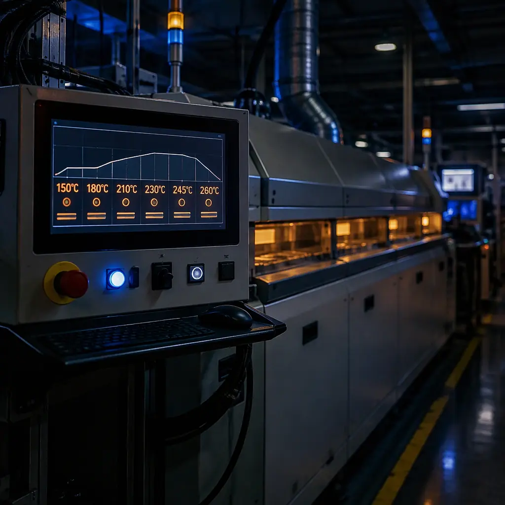
Design of experiments turns a reflow profile from a guess into a proven process window. How screening: characterisation and confirmation DOEs work
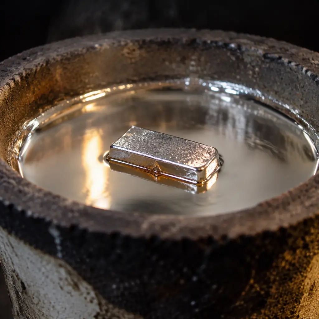
Solder float test and wetting balance both measure solderability but answer different questions. How each works: what the results mean
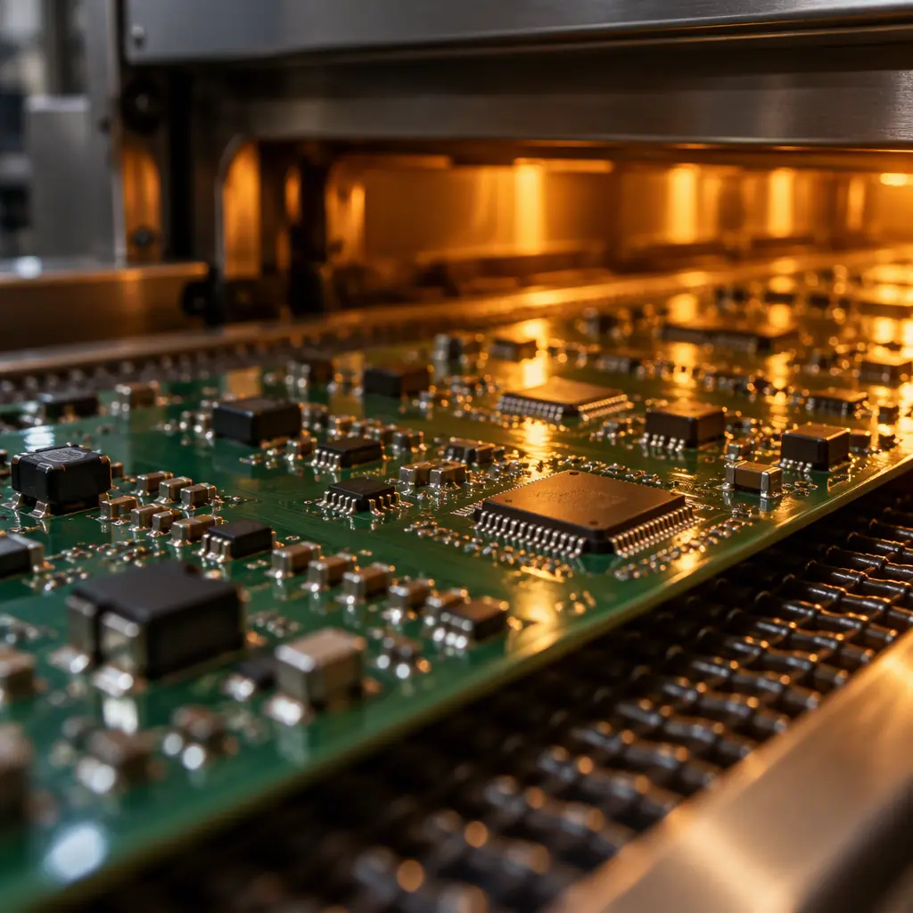
How to improve first pass yield in SMT assembly: the eight levers that actually move FPY, how to sequence them by payback
A structured method for assessing PCB supplier risk before you place the order: the eight dimensions that matter, how to score them
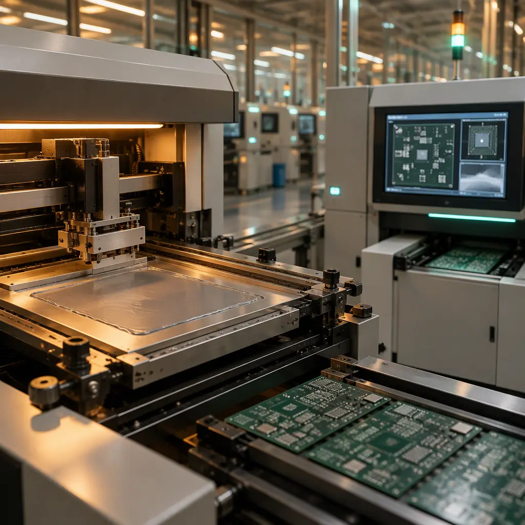
How to build a PCBA control plan and PFMEA: PCBA failure modes, the control-plan columns, a worked SMT-line example, and what buyers should demand at PPAP.
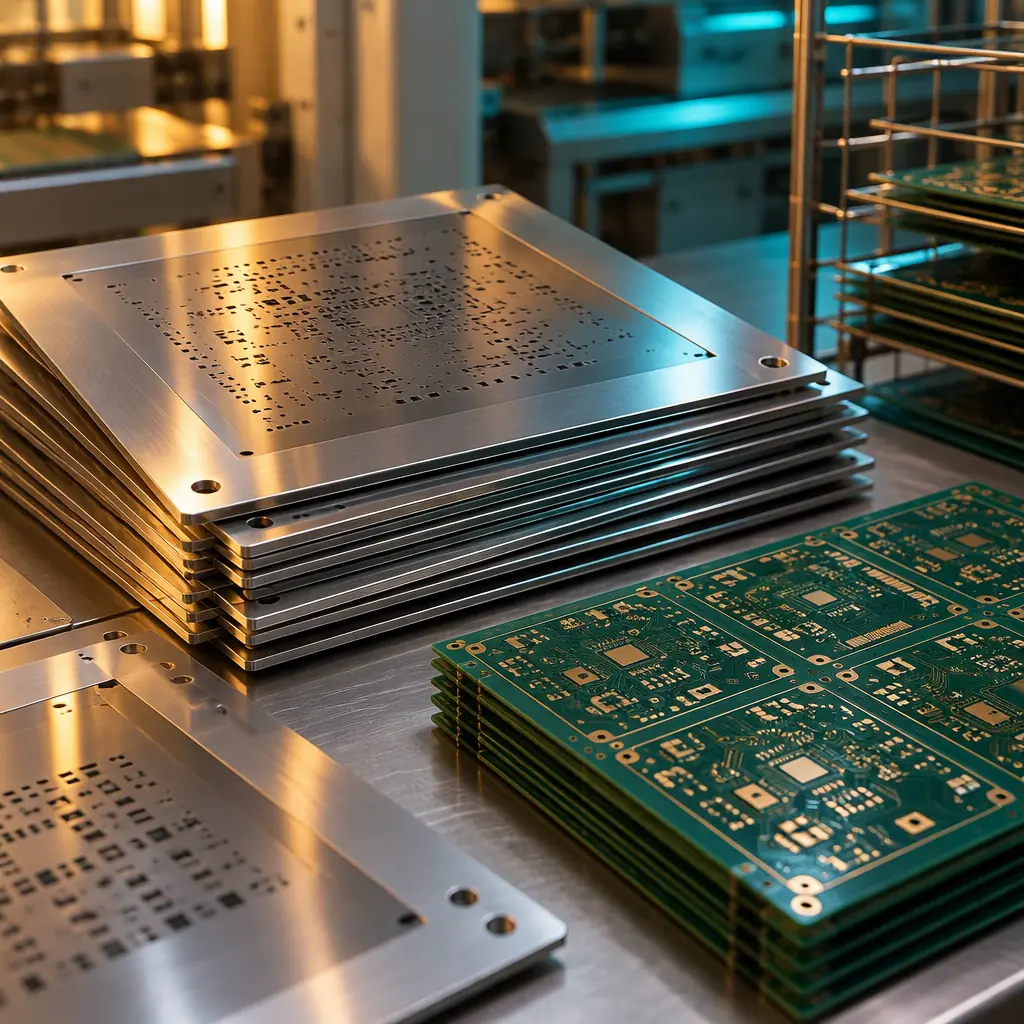
Who owns your Gerbers, stencils, test fixtures and source files — and the contract terms, escrow and exit checklist that keep your PCB manufacturing portable.

How grey-market and counterfeit parts reach production, and the incoming-inspection ladder — XRF, decap, DPA, AS6081 — buyers use to verify authenticity.
Upload your Gerber files and BOM. We'll respond within 24 hours with a detailed quote and free DFM review.