

Blog
Technical articles on PCB design, manufacturing, and industry best practices. Written by our engineering team.
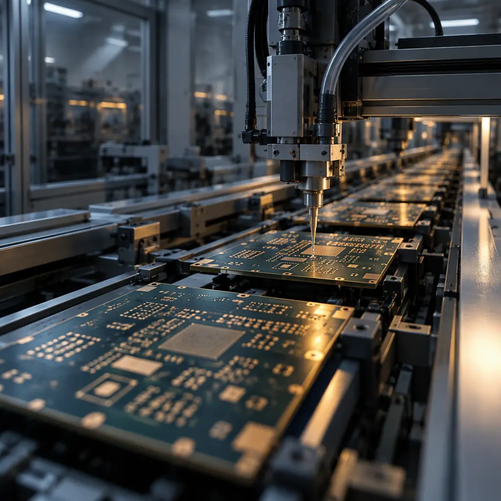
Stencil-free SMT line engineering, paste handling SOP, takt math and the staffing shift versus a stencil printer
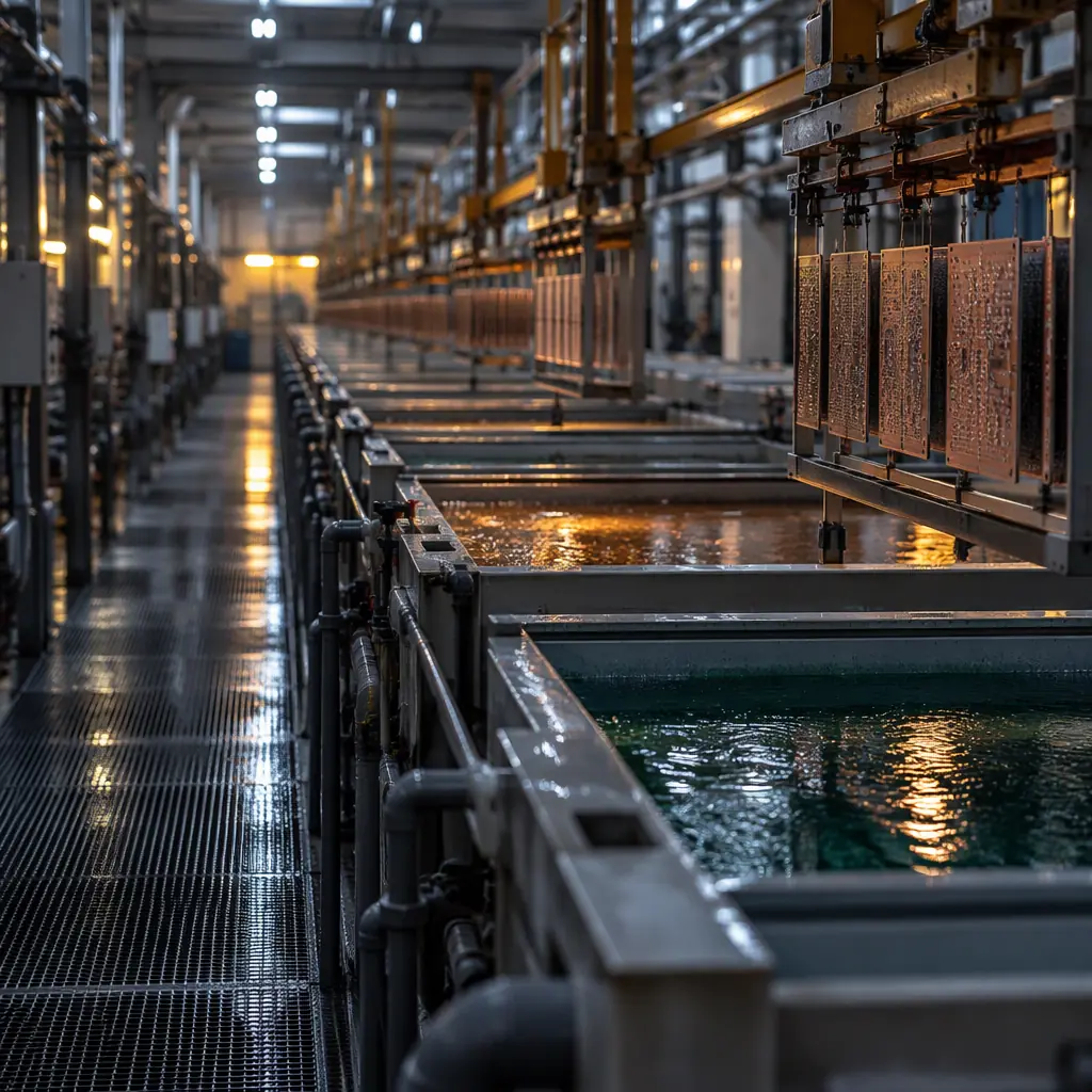
What carbon and ESG data a PCB supplier can actually provide: kWh per m2, product carbon footprint boundaries, Scope 2 and 3 reality
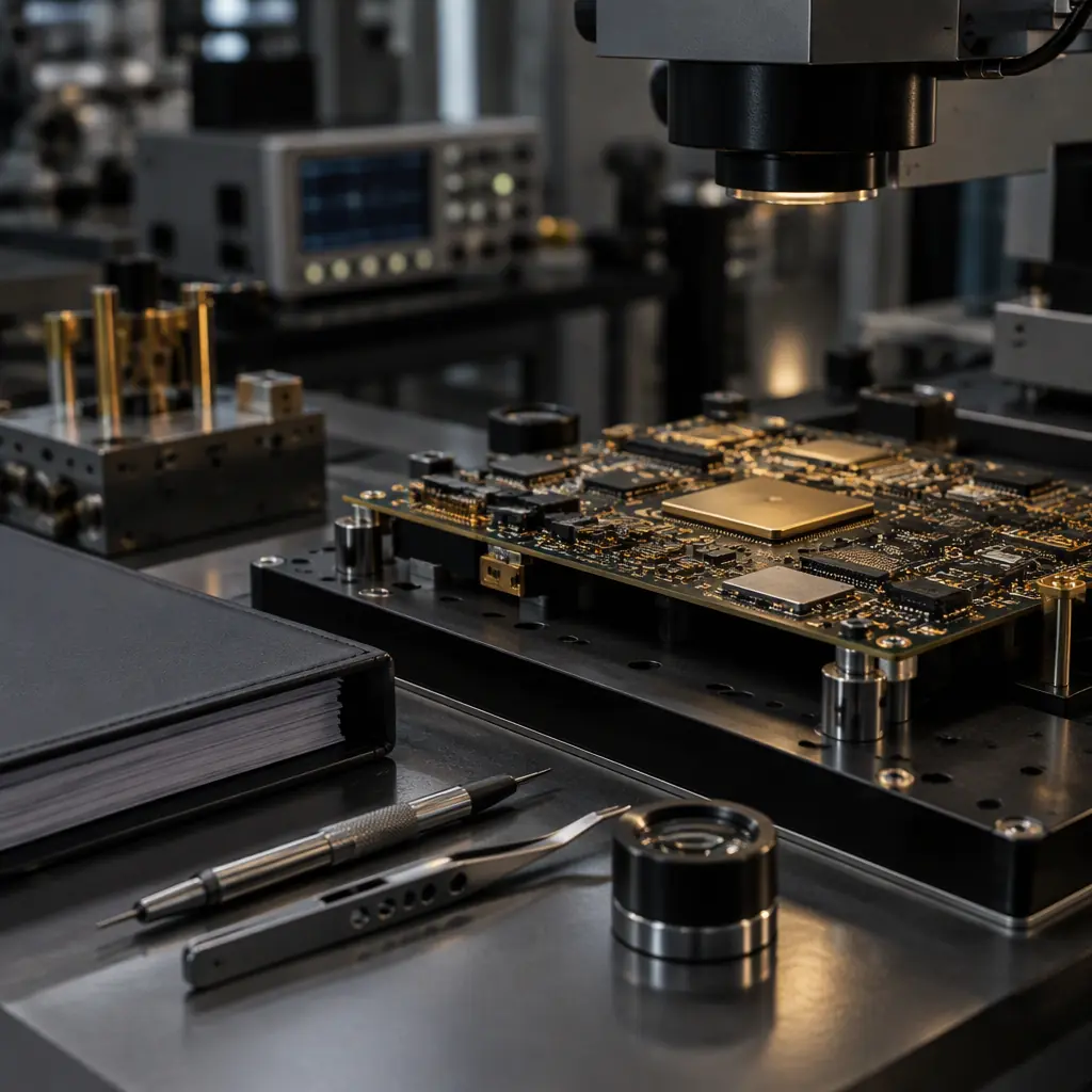
How to verify an AS9100D PCB supplier: certificate scope wording, OASIS lookup, AS5553 counterfeit controls, AS9102 FAI and the AS9100 versus ITAR distinction
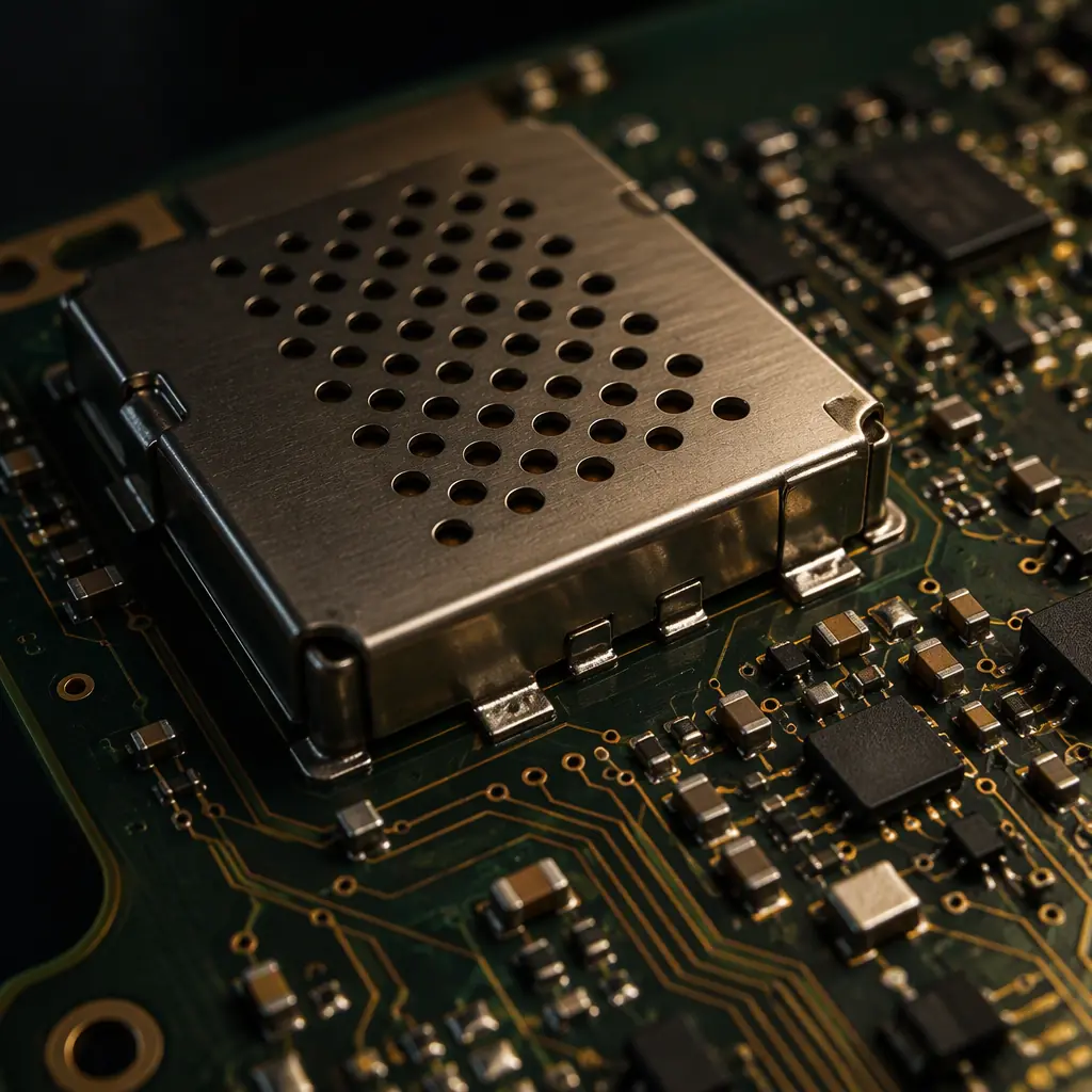
Board-level EMI shielding for PCBA: when to use a metal can vs a fence-and-lid: shielding effectiveness targets, gasket selection
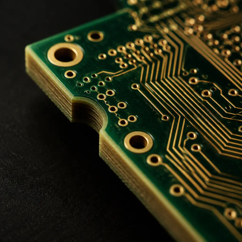
When to specify buried and blind vias in an HDI stackup: sequential lamination cost, aspect ratio limits
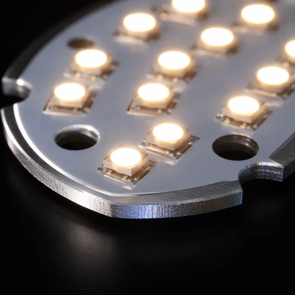
Aluminum and metal-core (IMS) PCB design rules: dielectric options, thermal path calculations, single-sided limits, LED and power applications
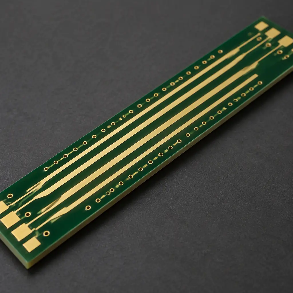
How to specify impedance test coupons and read the TDR report, sampling plans and the corrective loop when a coupon fails
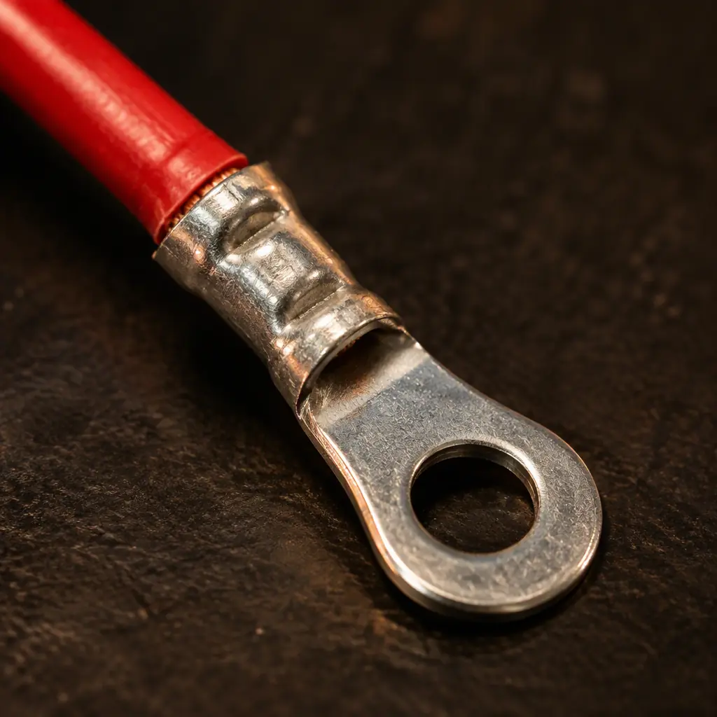
Crimp acceptance specs for cable harnesses: pull-force by wire gauge, micro-ohm and voltage-drop limits, continuity and hi-pot testing
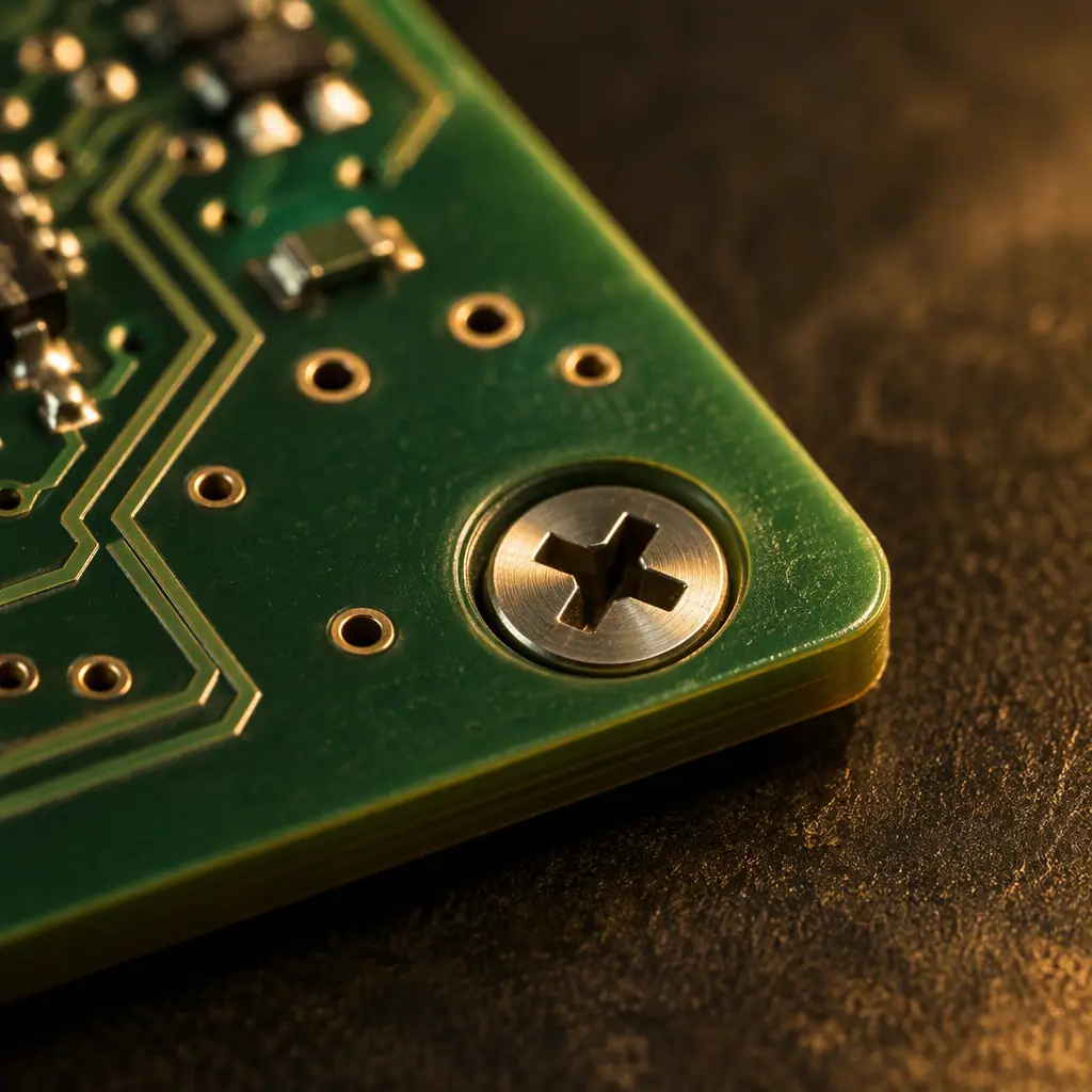
Design rules and real tolerances for countersinks: counterbores, depth routing and PCB cavities. What a Shenzhen fab can actually hold
Upload your Gerber files and BOM. We'll respond within 24 hours with a detailed quote and free DFM review.