

Blog
Technical articles on PCB design, manufacturing, and industry best practices. Written by our engineering team.
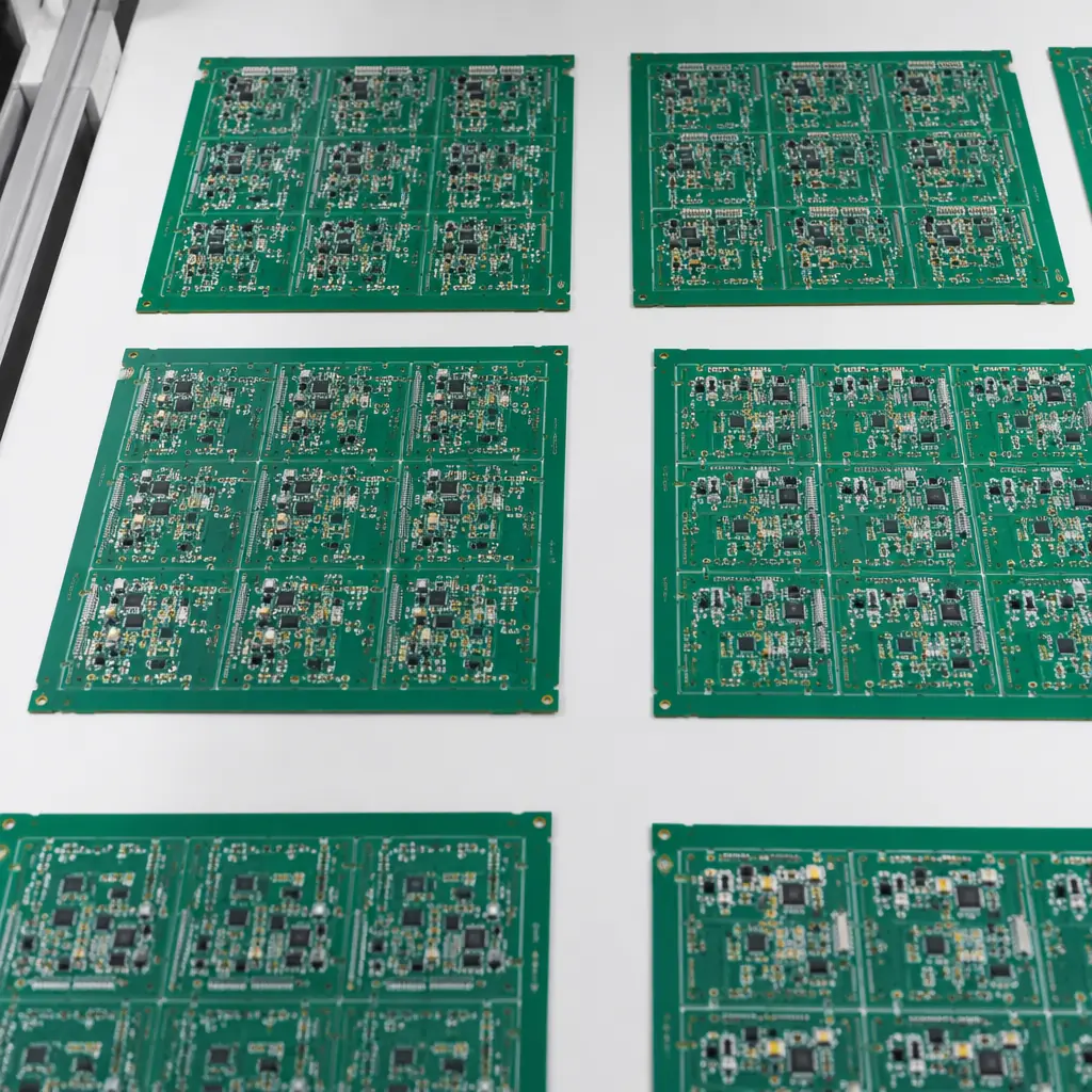
PCB panel utilization directly impacts your per-unit cost. Learn how rail width, nesting algorithms, V-score vs tab-routing, and mixed-panel strategies can redu

Complete engineering guide to PCBs for MWD/LWD tools, downhole sensors, and wellhead control systems. Covers 175-225°C materials (polyimide, ceramic, PTFE), H2S

Comprehensive guide to PCB manufacturing for optical transceiver modules (QSFP-DD, OSFP). Covers high-speed substrate requirements, ultra-low-loss materials, an
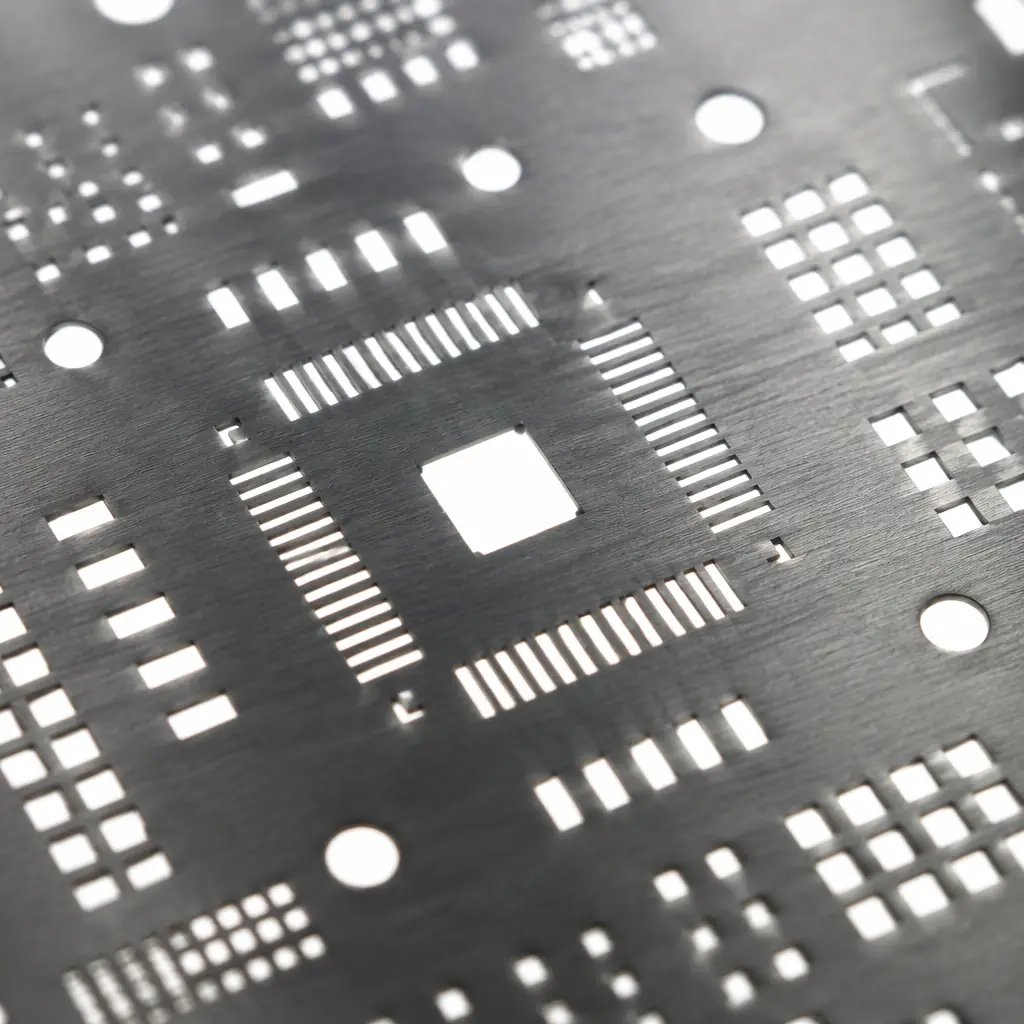
Complete guide to PCB NRE and tooling costs: setup charges, stencil fees, ICT/test fixture costs, programming fees, and how to budget NRE for prototype and prod
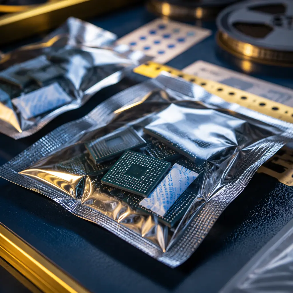
MSL classification determines whether your PCBs survive reflow or delaminate from trapped moisture. This guide covers MSL levels 1-6, floor life, baking require
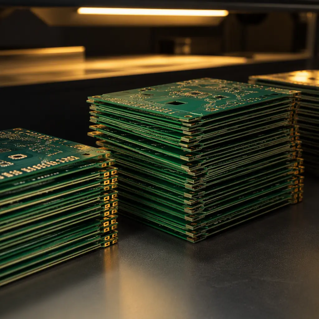
PCB MOQ explained — fabrication vs assembly vs component minimums, panel math, NRE tooling, and six strategies to lower your effective MOQ when sourcing PCBs fr
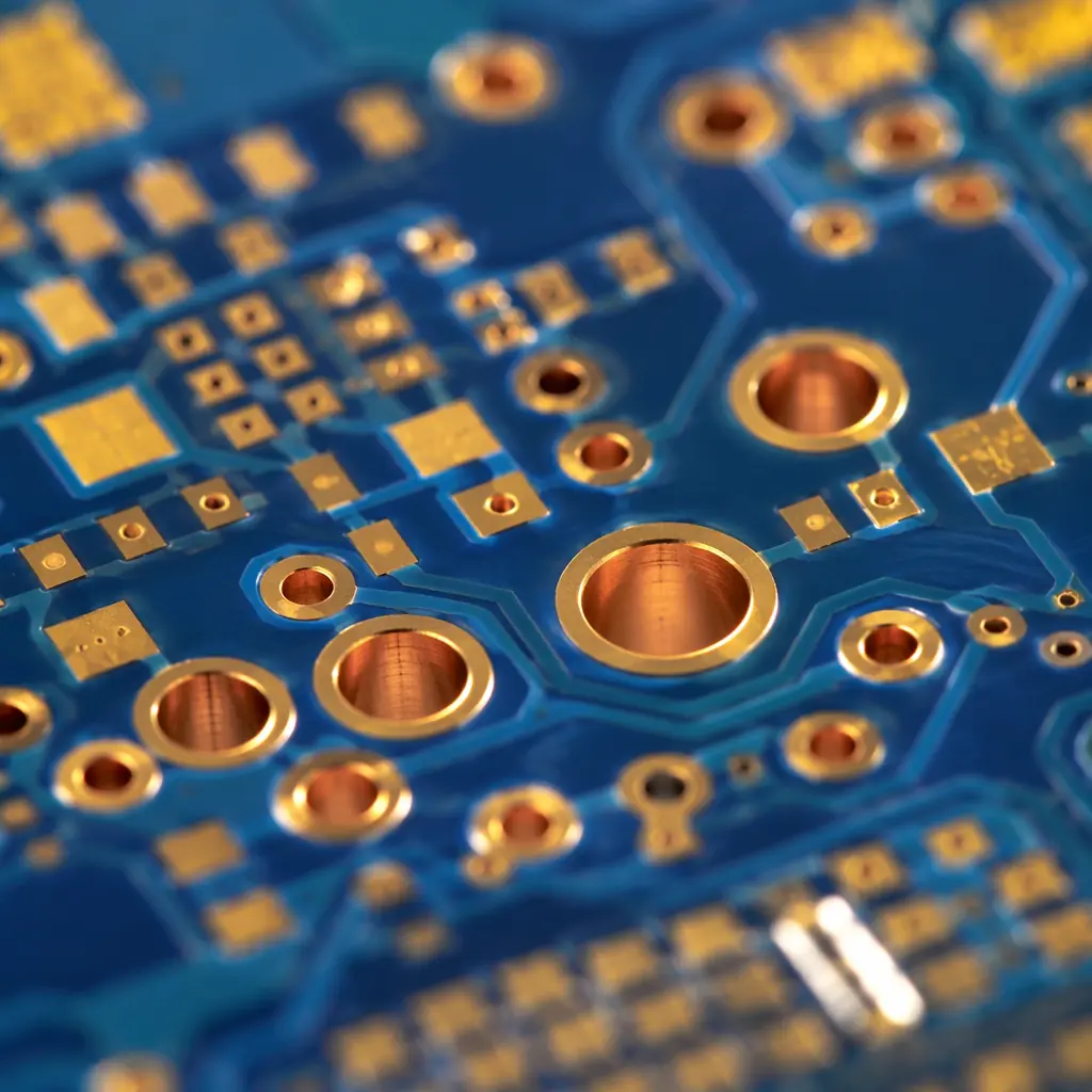
Complete engineering guide to PCB microvia reliability: stacked vs staggered configurations, IST testing methodology per IPC-TM-650, and IPC-6012 qualification
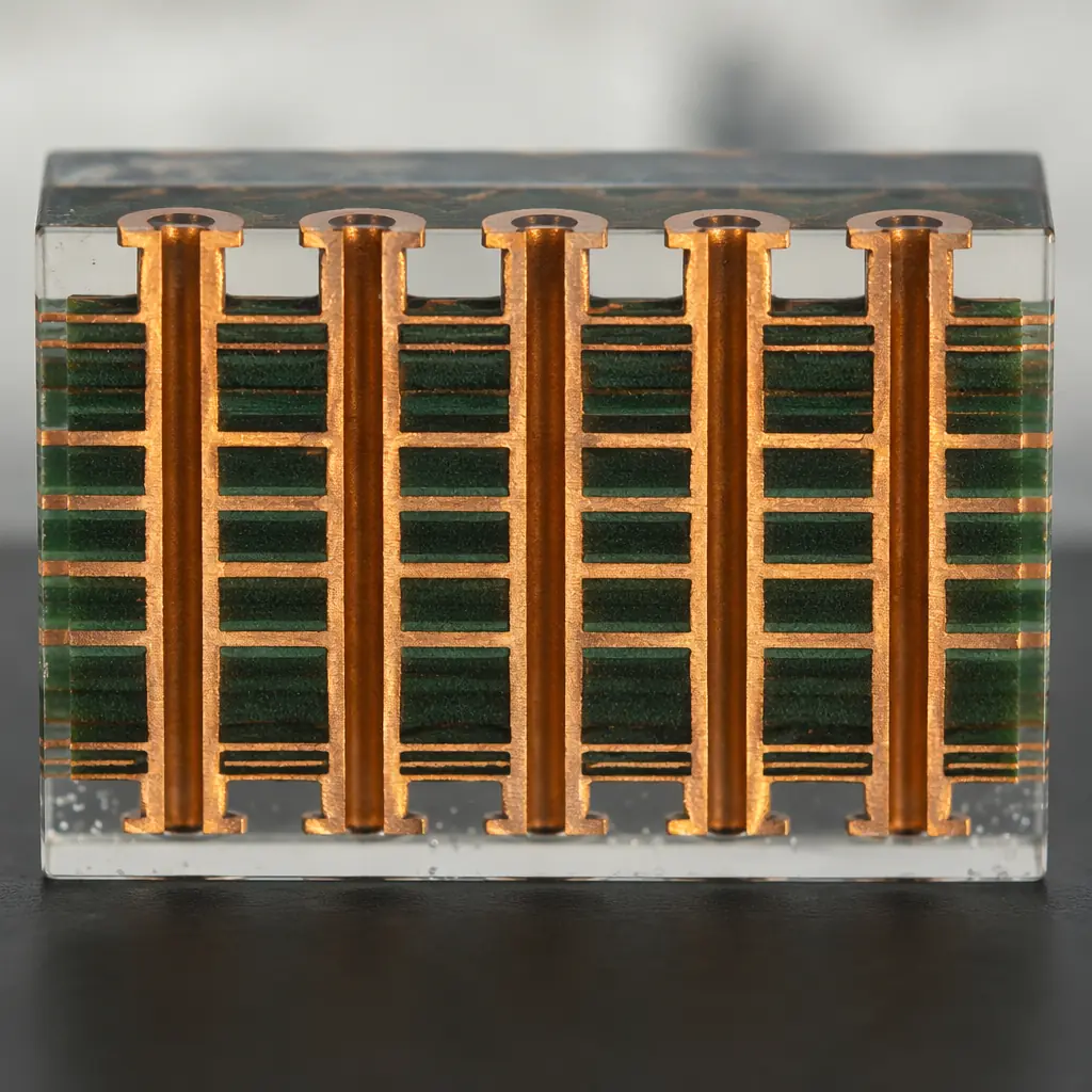
Complete guide to PCB microsection analysis: cross-section preparation, potting, polishing, and microscope measurement of copper barrel thickness, IMC layer, vi
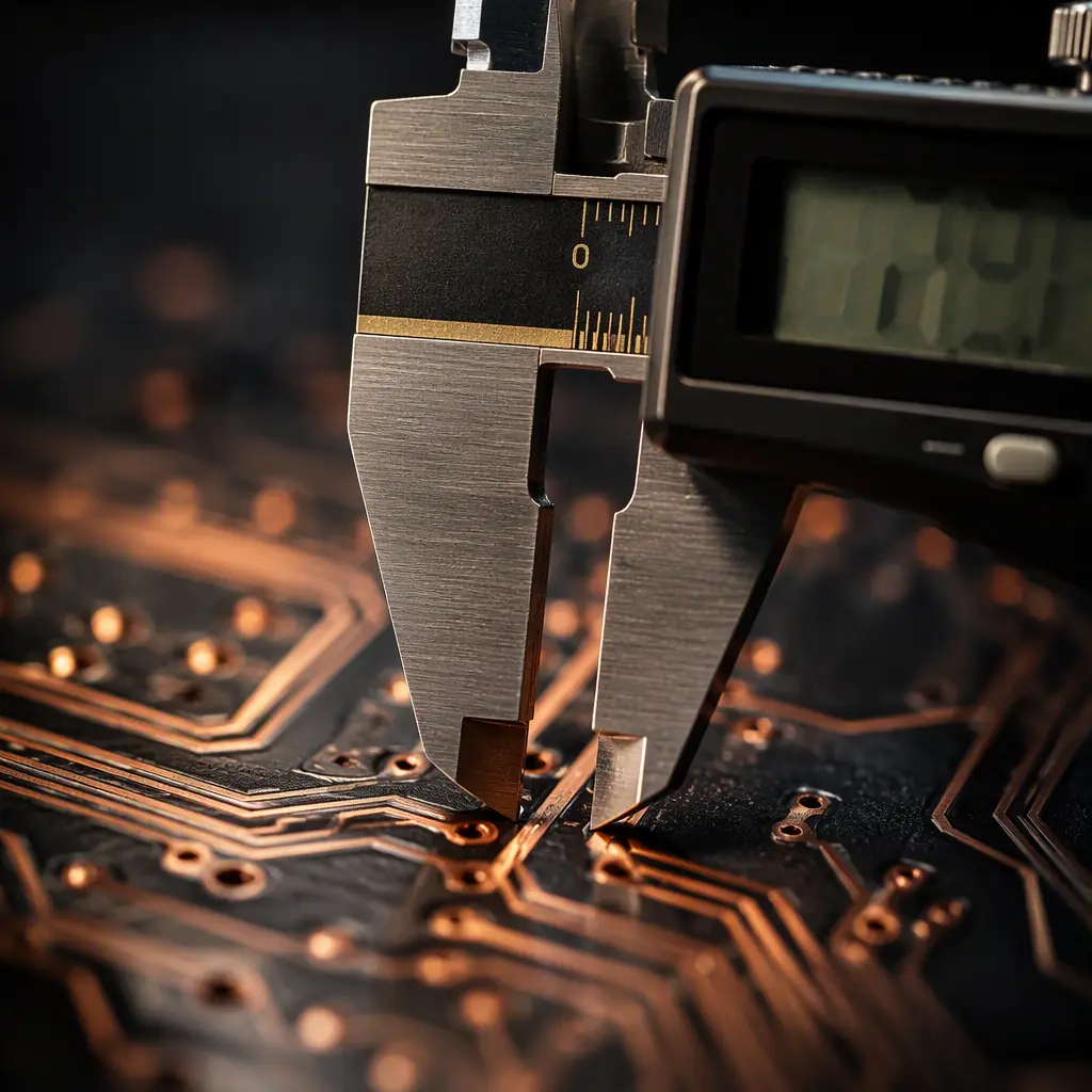
PCB manufacturing tolerances explained for design and procurement engineers — standard vs tight limits for trace width, drill, annular ring, registration, imped
Upload your Gerber files and BOM. We'll respond within 24 hours with a detailed quote and free DFM review.