

Blog
Technical articles on PCB design, manufacturing, and industry best practices. Written by our engineering team.
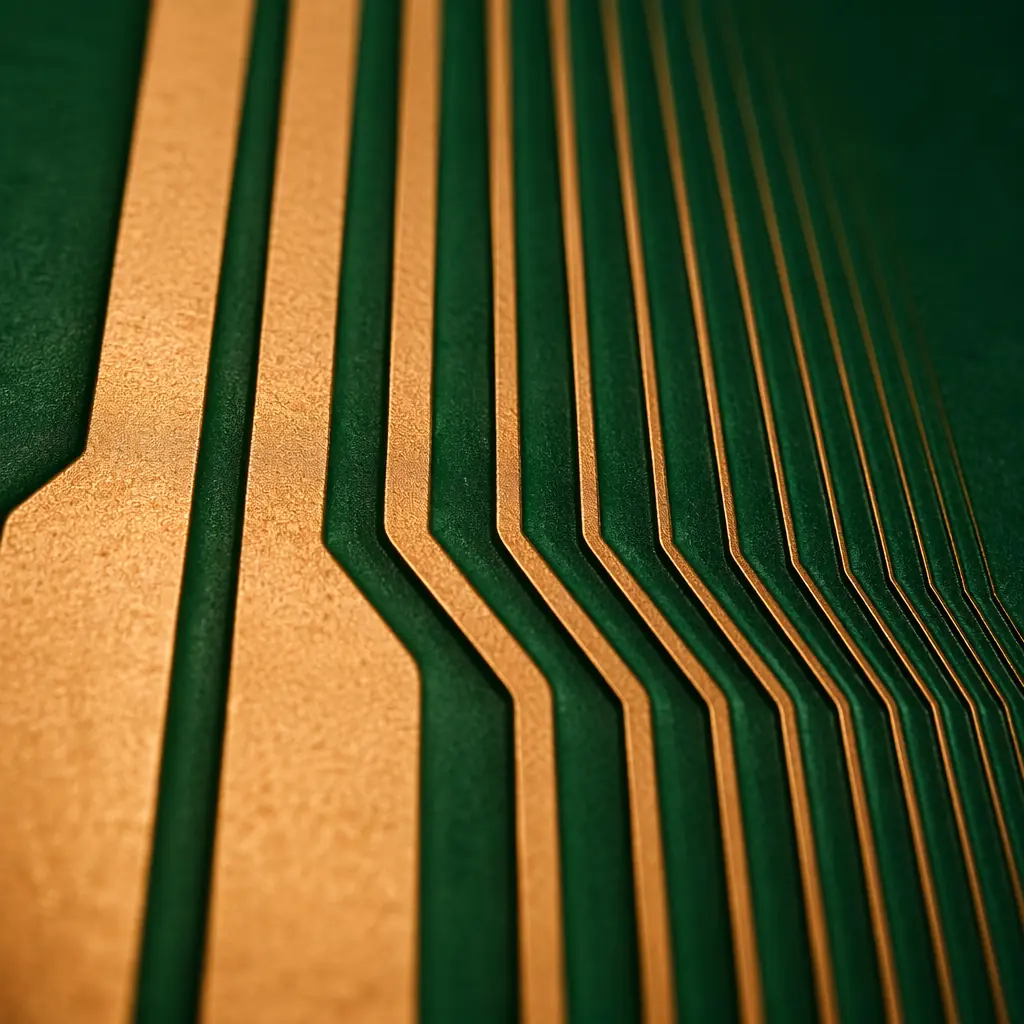
Complete guide to PCB trace width calculation for current carrying capacity. IPC-2152 vs IPC-2221 comparison: copper weight vs trace width charts
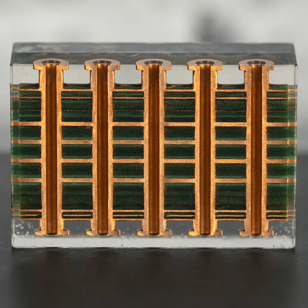
Complete guide to PCB microsection analysis: cross-section preparation, potting, polishing, and microscope measurement of copper barrel thickness, IMC layer

Complete guide to PCB ionic contamination and cleanliness testing: ROSE (IPC-TM-650 2.3.25), SIR (Surface Insulation Resistance), ion chromatography
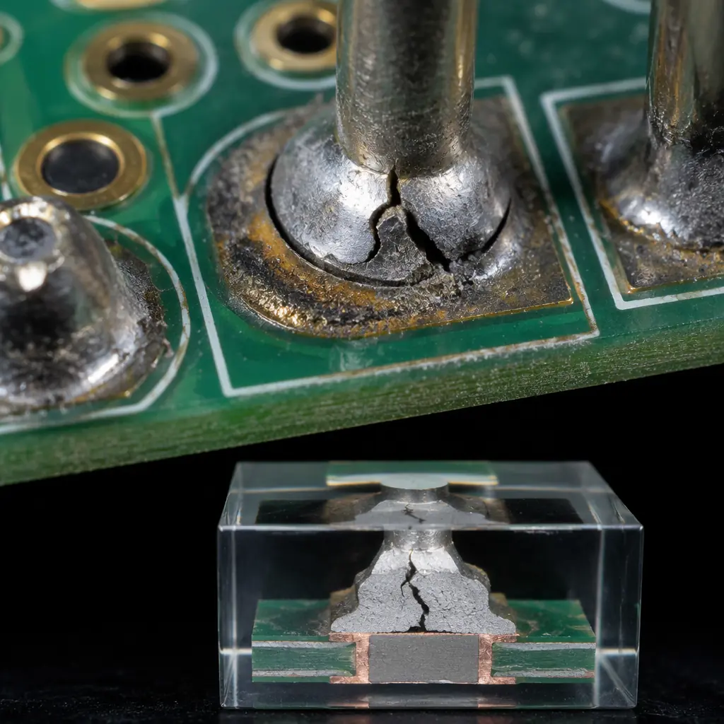
Complete PCB failure analysis guide, and solder joint reliability analysis. How to investigate PCB failures and prevent recurrence
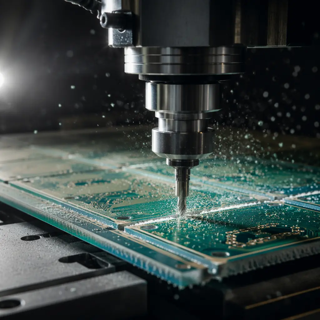
Comprehensive comparison of PCB depaneling methods, and design rules for each method. How to choose the right singulation process for your PCB
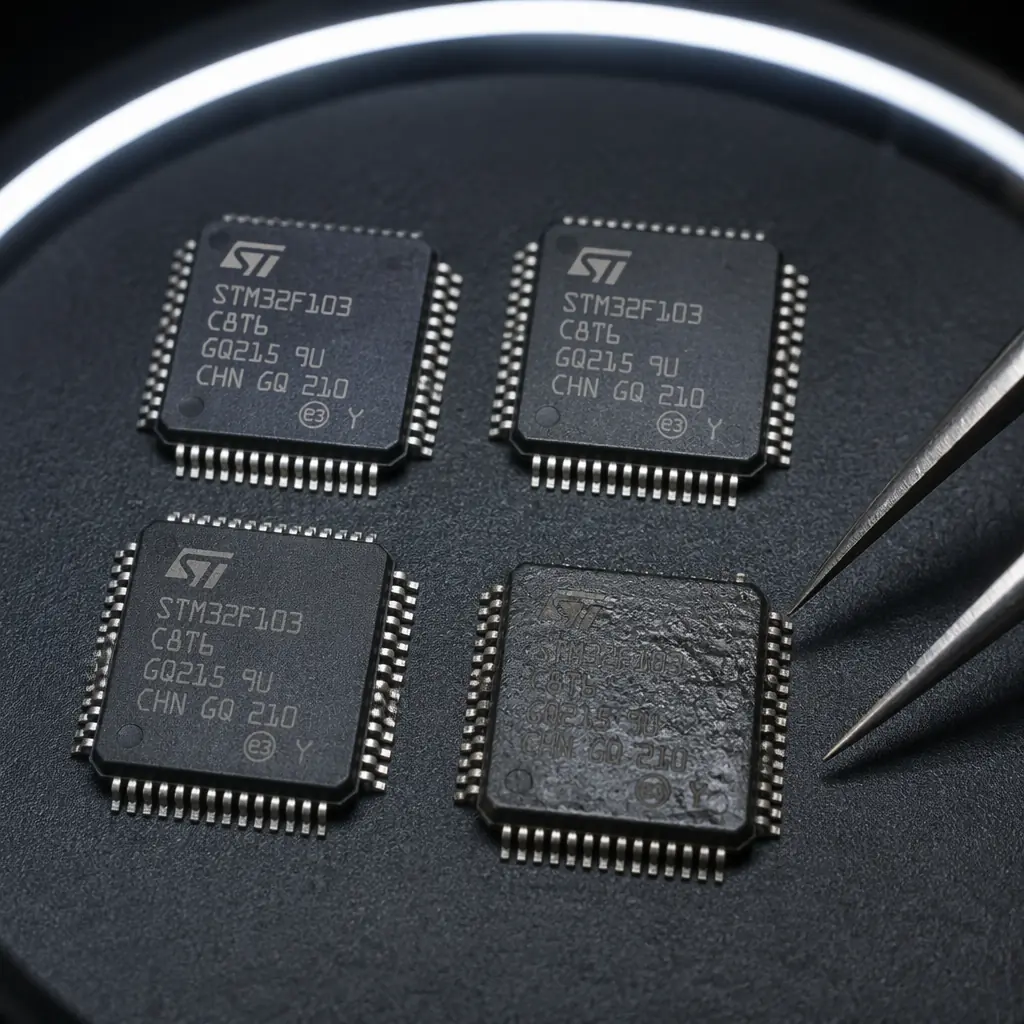
How to detect counterfeit PCBs and electronic components: blacktopping visual inspection, X-ray internal comparison, decapsulation, XRF material verification
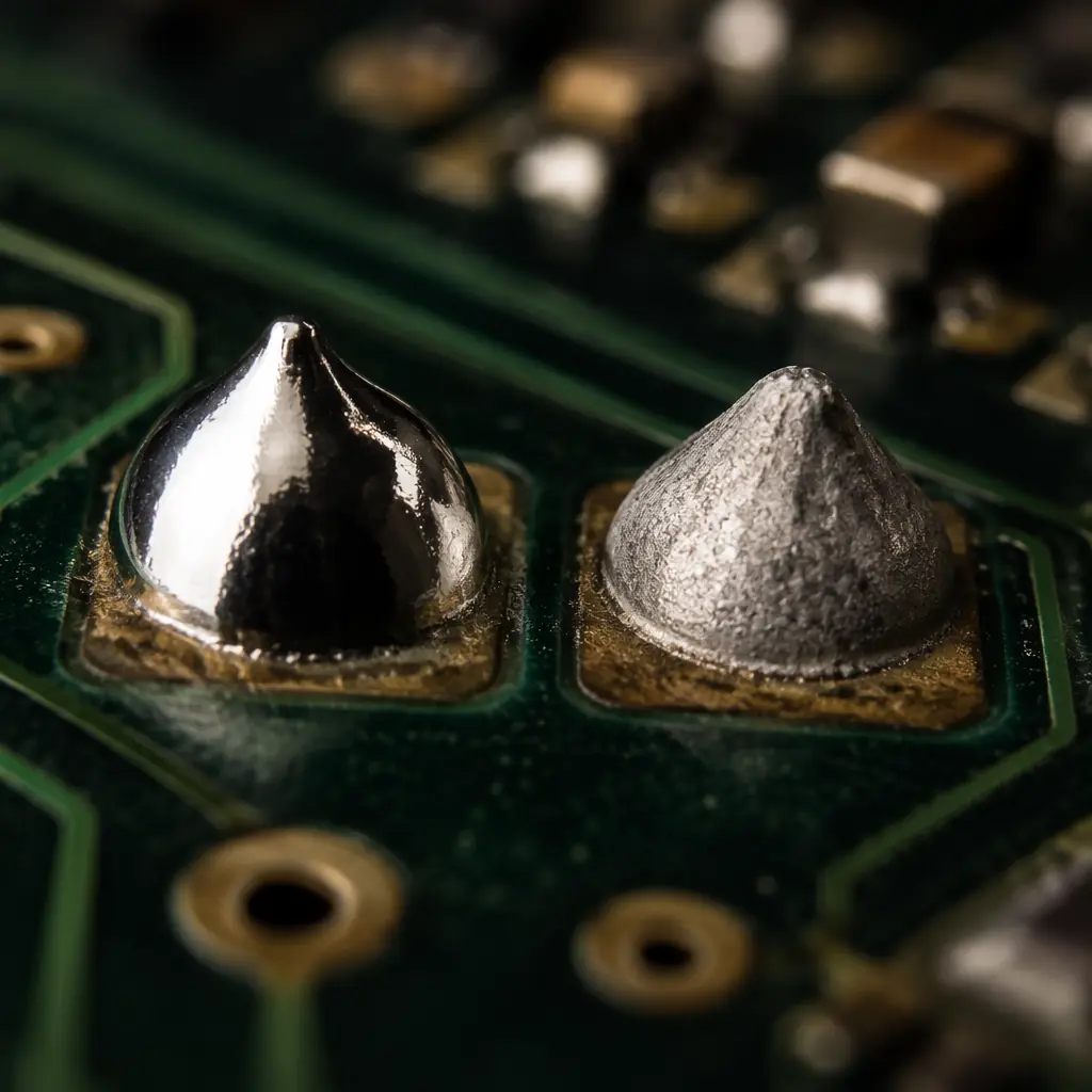
Data-driven comparison of lead-free (SAC305: SN100C) vs leaded (SnPb) solder for PCB assembly. Reliability testing results, tin whisker mitigation strategies
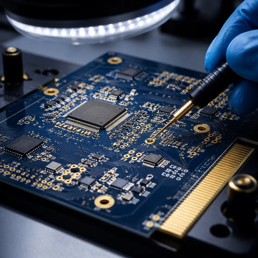
Complete IPC-A-600 acceptance criteria guide for PCB buyers. Class 1/2/3 inspection standards plus how to read inspection reports and verify supplier
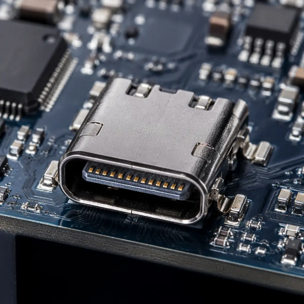
Complete USB-C PCB design guide for hardware engineers: 90Ω differential impedance routing, SuperSpeed lane layout, ESD protection placement
Upload your Gerber files and BOM. We'll respond within 24 hours with a detailed quote and free DFM review.