

Blog
Technical articles on PCB design, manufacturing, and industry best practices. Written by our engineering team.
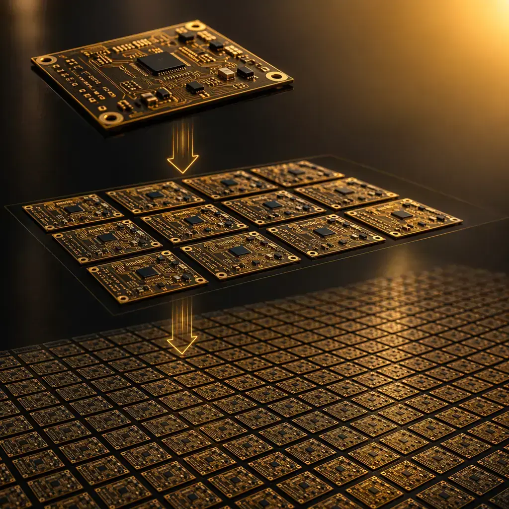
Real cost breakdown of PCB prototyping vs mass production. How quantity: panel utilization, NRE amortization, and yield affect per-unit cost. See the math
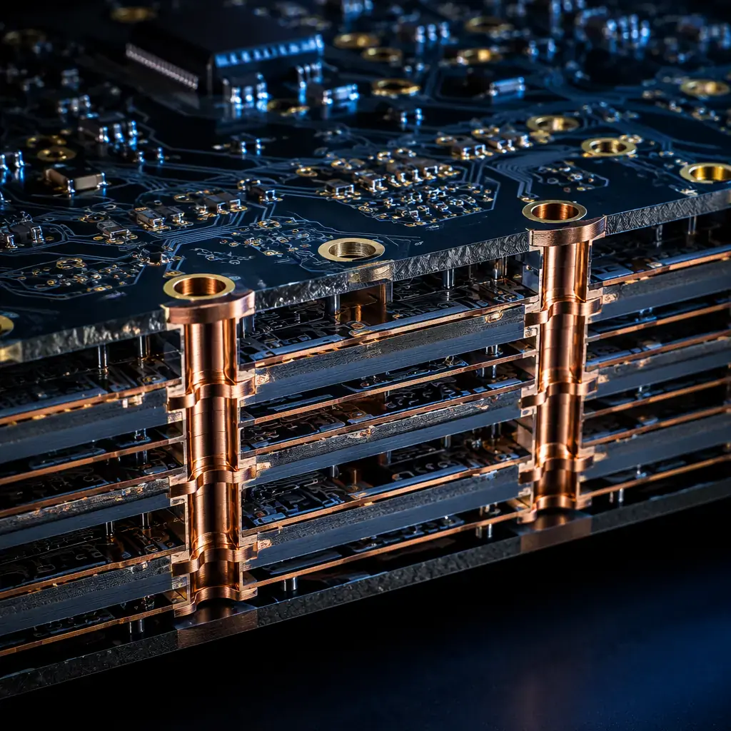
Complete guide to PCB via types: through-hole vs blind vs buried vias, via-in-pad design rules, backdrilling for signal integrity
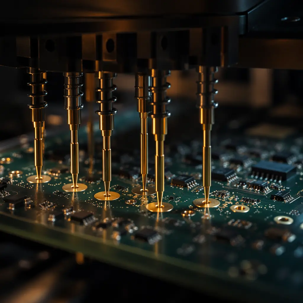
Complete comparison of PCB testing methods: AOI vs X-Ray vs Flying Probe vs ICT vs Functional Test. What each method catches, what it misses, when to use each
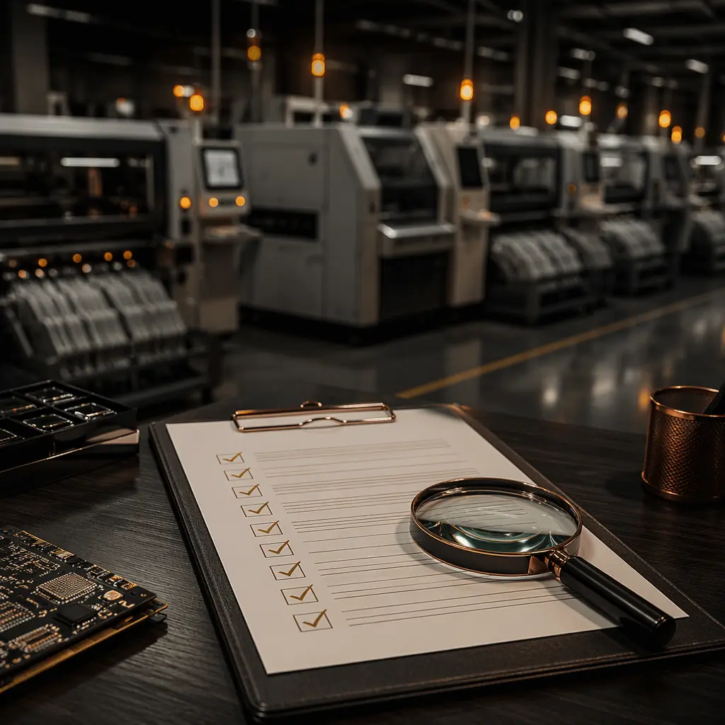
A practical 10-point checklist for evaluating Chinese PCB manufacturers. Factory audit questions: certification verification
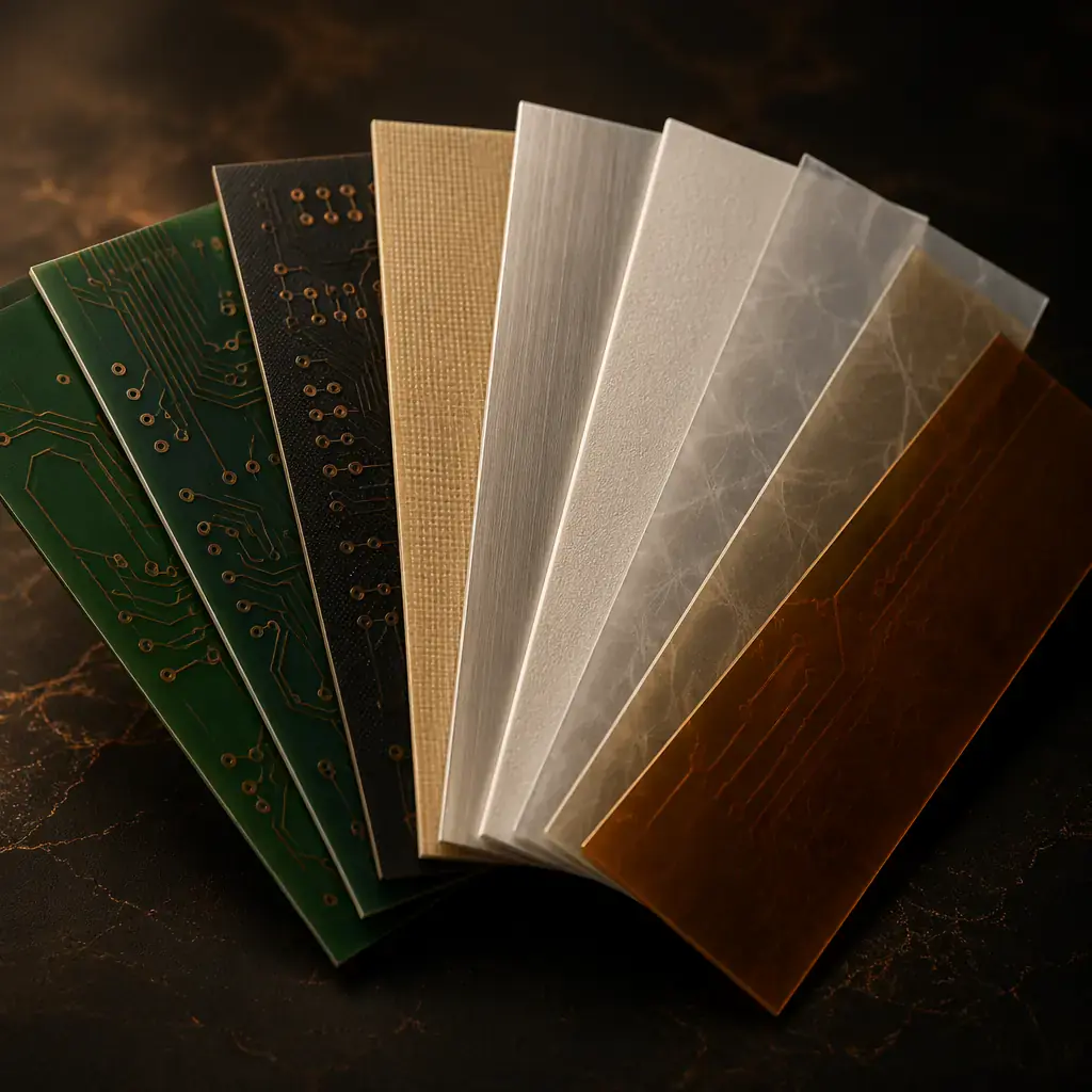
FR-4: High-Tg, Rogers, aluminum, ceramic, PTFE, polyimide, which PCB substrate is right for your design? Compare Tg, Dk, thermal conductivity
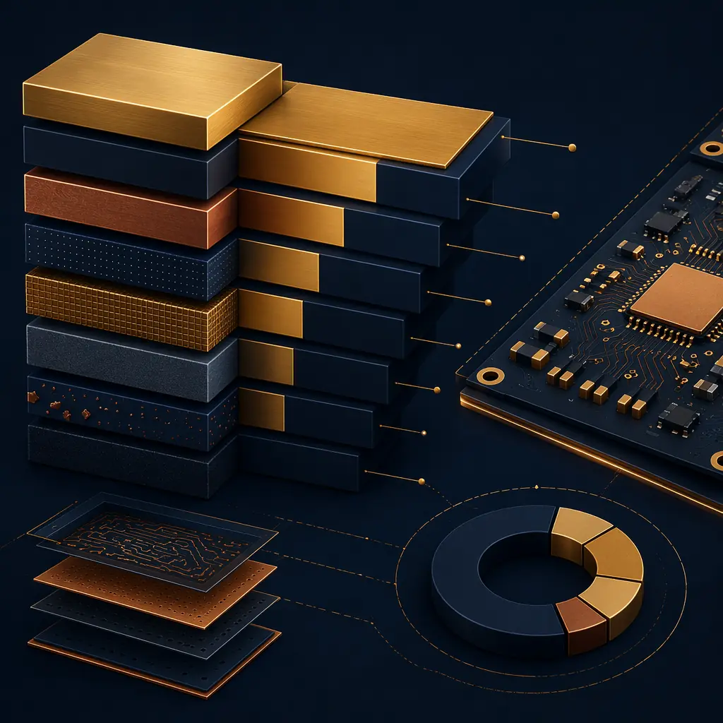
Complete breakdown of what drives PCB manufacturing cost: layer count, materials, surface finish, volume
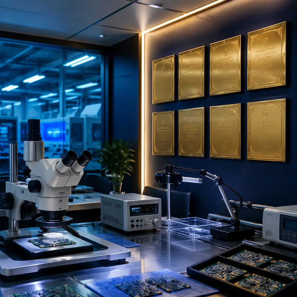
Complete buyer's guide to PCB certifications: ISO 9001, IATF 16949, UL 94 V-0, IPC-A-610 Class 3, RoHS, REACH — what each standard means
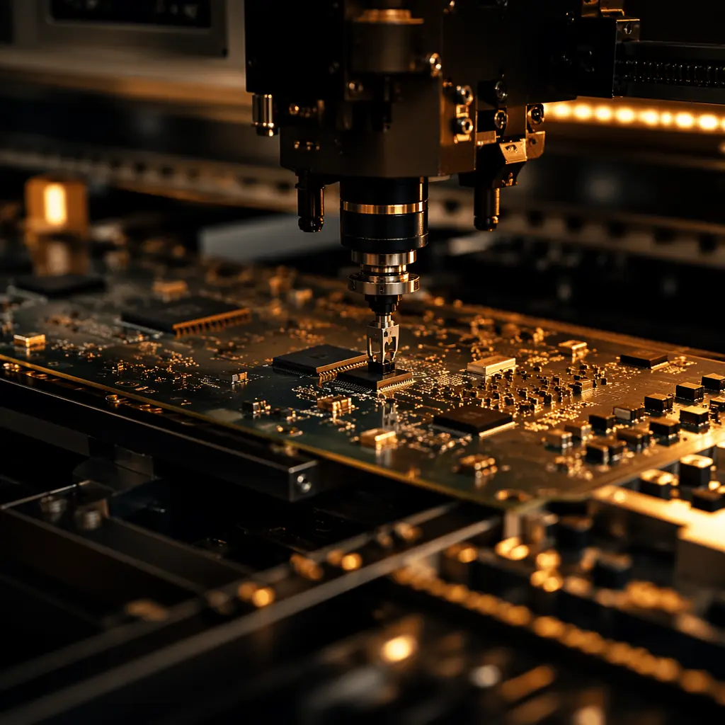
Complete PCB assembly process explained: solder paste printing, SMT placement, reflow soldering, AOI inspection, through-hole assembly
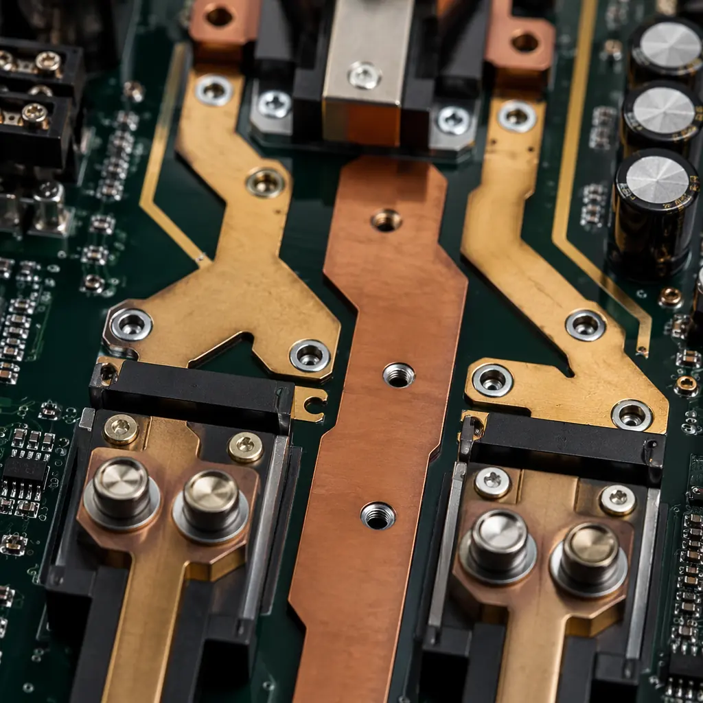
Technical PCB requirements for new energy applications: EV charging stations, battery energy storage systems, and solar inverters. High-current copper
Upload your Gerber files and BOM. We'll respond within 24 hours with a detailed quote and free DFM review.