

Blog
Technical articles on PCB design, manufacturing, and industry best practices. Written by our engineering team.
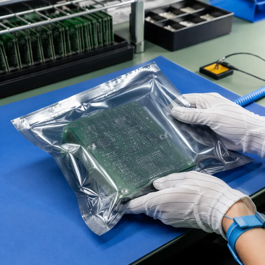
Complete guide to PCB ESD packaging and shipping standards: IPC-1601 requirements, moisture barrier bags, vacuum sealing, desiccant specifications, and humidity

PCB requirements for AC Level 2 and DC fast charging stations: high-current power distribution, thermal management for 350kW+ chargers, galvanic isolation, and
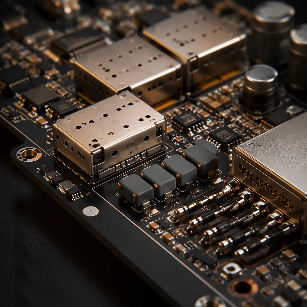
Complete PCB EMI/EMC design guide: stackup strategies, ground plane design, shielding, filtering, and pre-compliance testing. Pass FCC Part 15 and CE EN 55032 o

ESD control program requirements for PCB assembly per ANSI/ESD S20.20 — HBM/CDM damage models, EPA grounding, ionizers, packaging per ESD S541, and a 10-point s
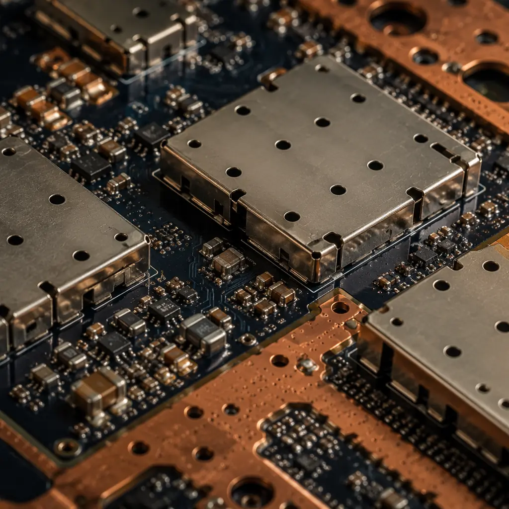
EMC compliance failures cost PCB buyers $15,000-$50,000 per redesign cycle. This guide covers the 5 PCB design decisions that determine whether your board passe
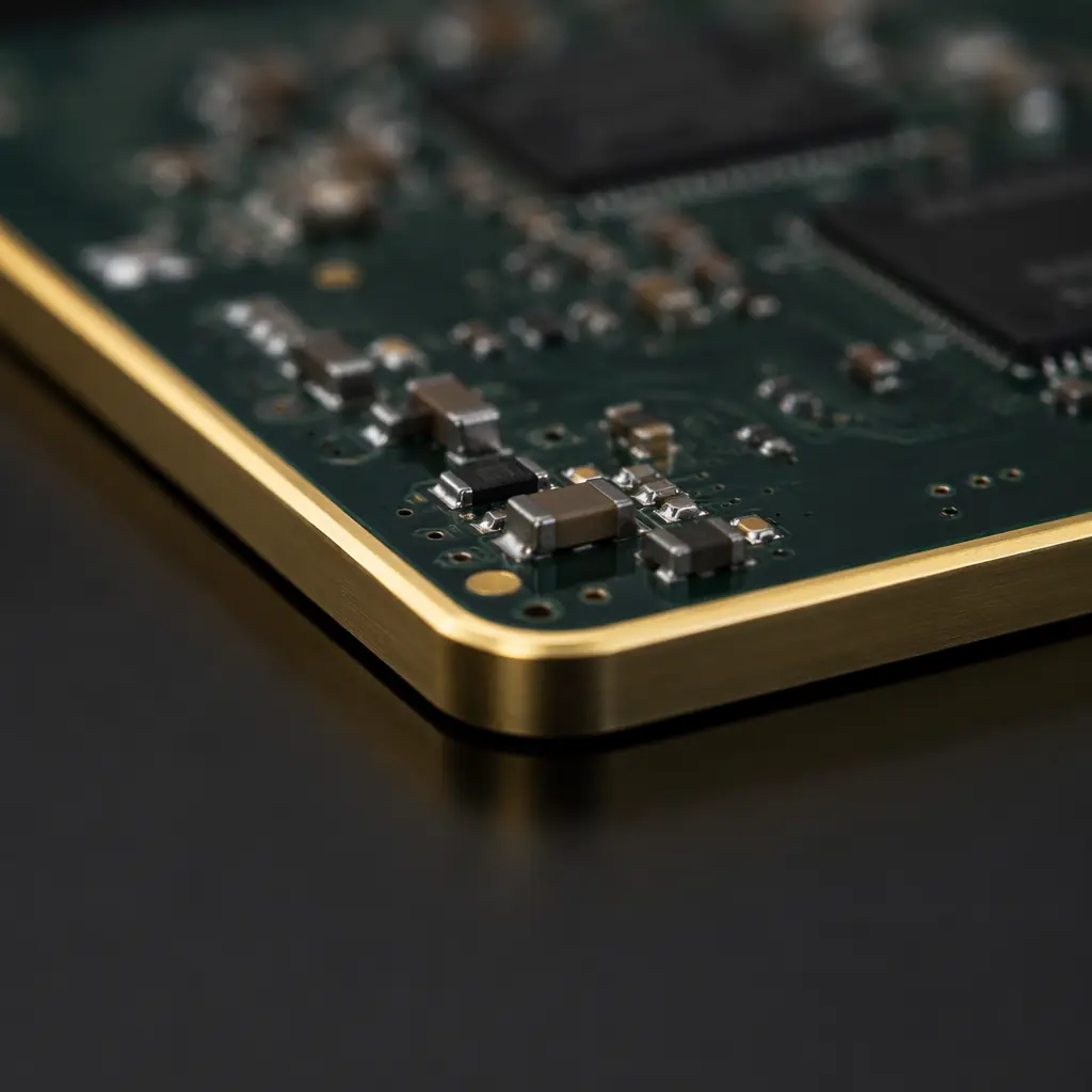
Complete PCB edge plating and castellated holes design guide: when to use sidewall metallization vs half-holes, minimum web specs, copper-to-edge clearance, pla
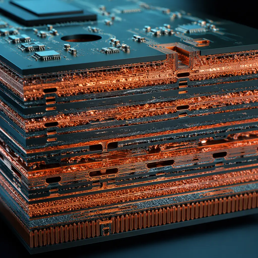
When should you replace discrete SMD passives with embedded components inside PCB layers? Compare planar capacitance, buried resistors, and trade-offs in cost,

How to qualify and manage multiple PCB assembly suppliers without quality drift. Supplier scorecard framework, dual-sourcing cost model, transition planning, an

Comprehensive comparison of PCB depaneling methods: router, V-score, laser, and punching. Edge quality, stress analysis, cost per panel, and design rules for ea

Upload your Gerber files and BOM. We'll respond within 24 hours with a detailed quote and free DFM review.