

Blog
Technical articles on PCB design, manufacturing, and industry best practices. Written by our engineering team.

UPS PCB design guide covering static bypass and heavy-copper thermal management for reliable uninterruptible power

LiDAR PCB design guide covering high-speed point-cloud data paths and thermal management for automotive and robotics sensors

Access control system PCB design: multi-door controller layout, Wiegand and OSDP reader interfaces, electric lock outputs
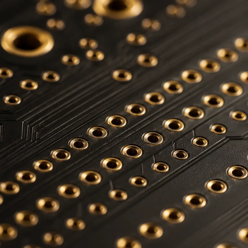
Drilled hole size: position accuracy and annular ring requirements explained, IPC-6012 tolerance classes
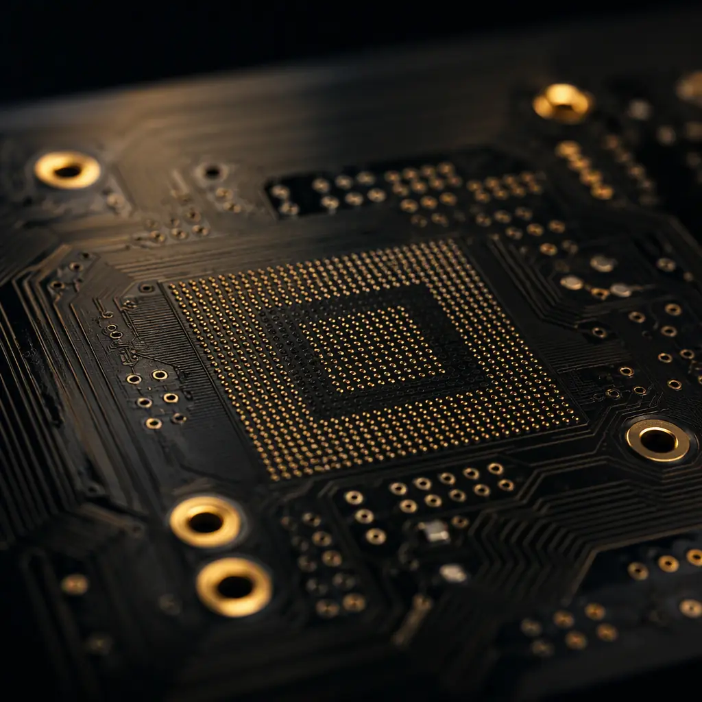
Copper-filled, resin-filled and conductive-paste vias explained: IPC-4761 types, via-in-pad rules, cost impact and DFM guidance for BGA and HDI boards.
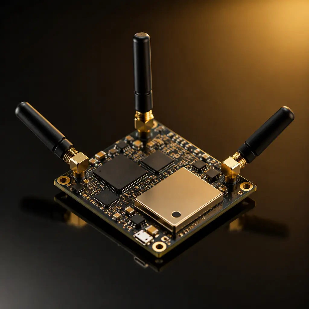
Multi-radio positioning module PCB design: GNSS + UWB + BLE AoA coexistence, antenna separation, power integrity and RTLS hardware integration guide.

Solder paste jetting vs stencil printing, accuracy and lead-time comparison for prototype and low-volume PCBA. When zero-tooling SMT actually saves you money
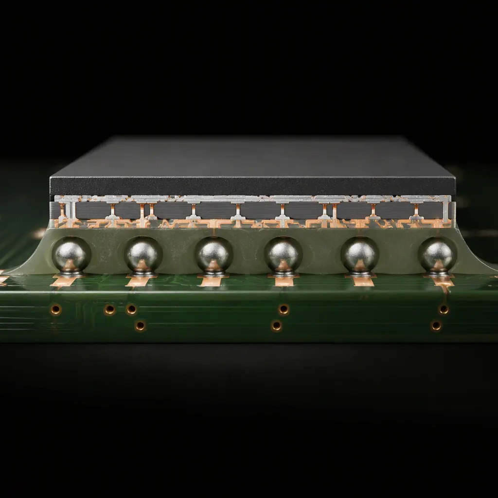
Underfill process guide for BGA, CSP and flip-chip: capillary vs no-flow vs molded underfill, material selection, void control and reliability testing.

Design for Assembly (DFA) rules for PCBA: component selection, footprint design, panelization and test access choices that reduce assembly cost and rework.

Upload your Gerber files and BOM. We'll respond within 24 hours with a detailed quote and free DFM review.