

Blog
Technical articles on PCB design, manufacturing, and industry best practices. Written by our engineering team.
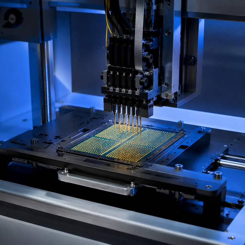
Technical sourcing guide for ATE load boards, probe cards, and burn-in boards: 40+ layer stackups, ±5% impedance tolerance, polyimide/BT/ceramic materials, via-

AQL sampling for PCB and PCBA inspection — how to read ISO 2859-1 / ANSI Z1.4 tables, choose inspection level and defect classes, and set AQL limits that match
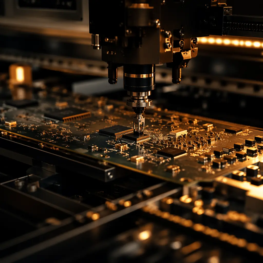
Complete PCB assembly process explained: solder paste printing, SMT placement, reflow soldering, AOI inspection, through-hole assembly, and functional testing.
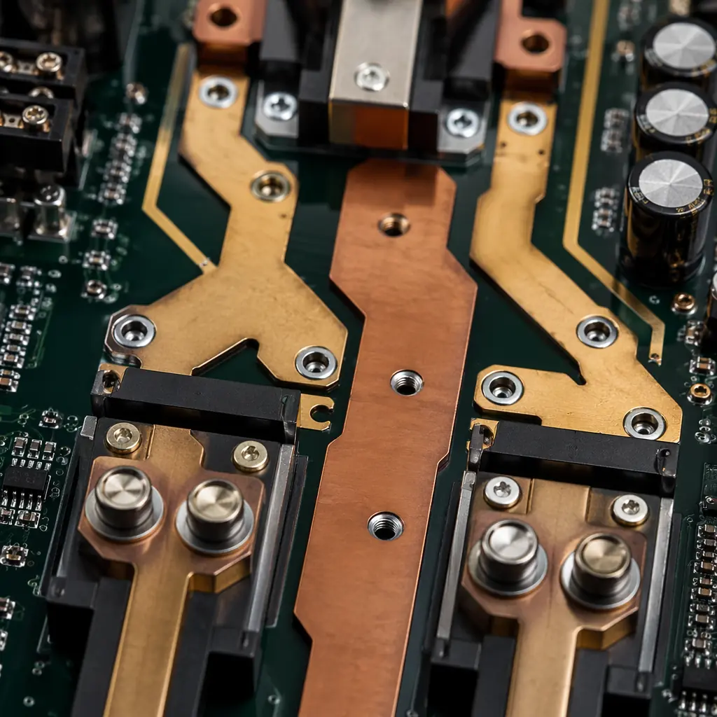
Technical PCB requirements for new energy applications: EV charging stations, battery energy storage systems, and solar inverters. High-current copper, thermal
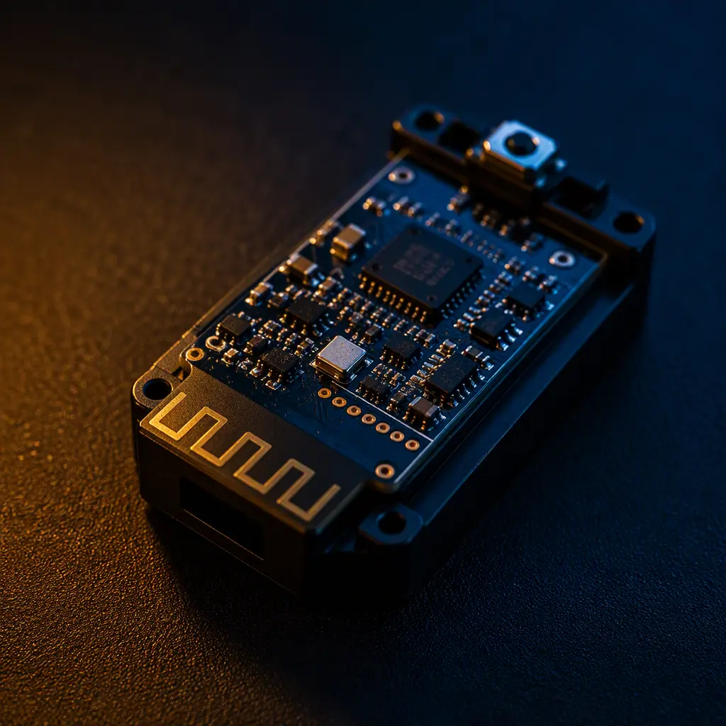
PCB antenna design guide — IFA and MIFA trace antennas, chip antennas, 50 ohm matching networks and tuning with a VNA, layout rules that preserve range, testing
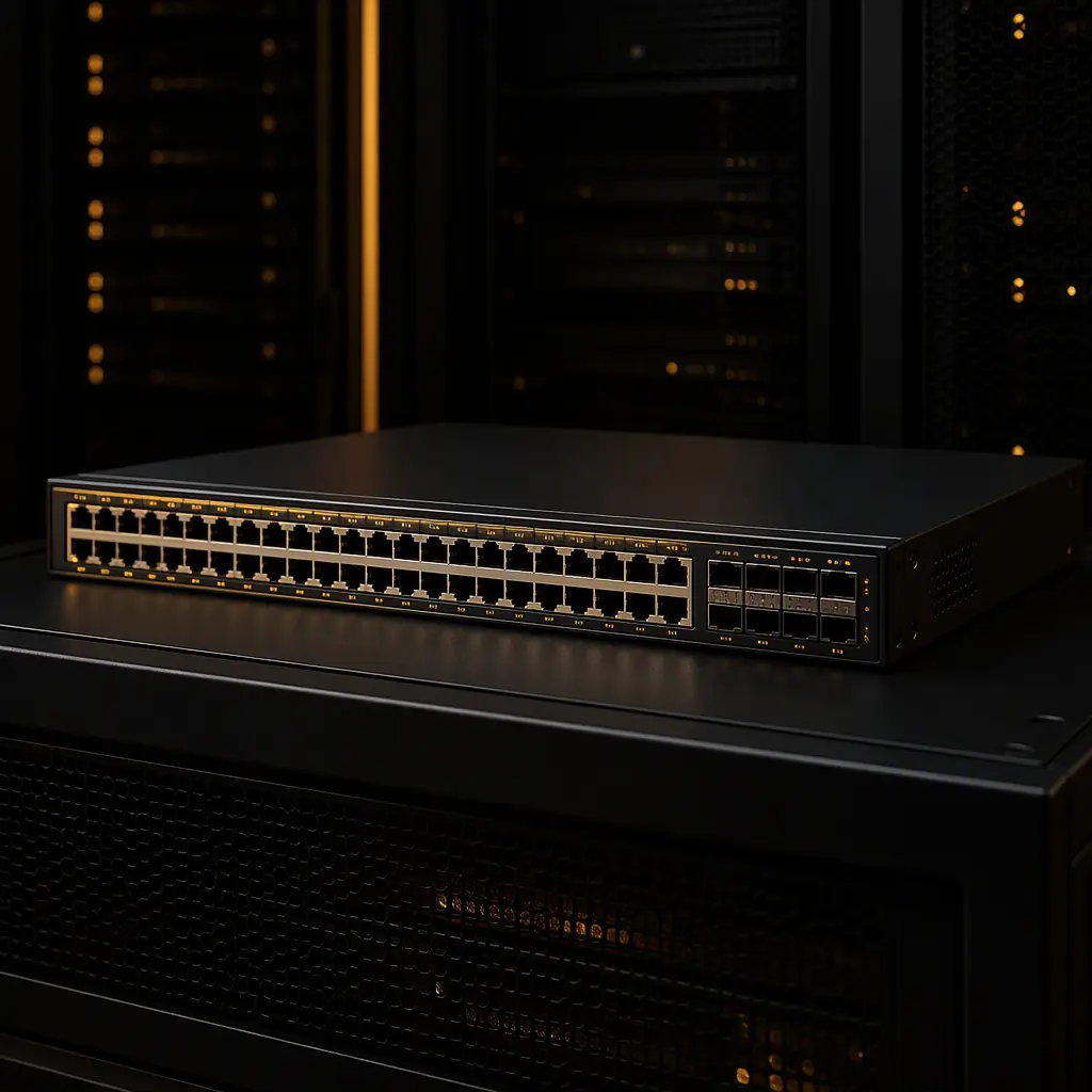
Engineering guide to network switch and router PCB manufacturing: 100G/400G Ethernet SerDes routing, 16-32 layer stackups, low-loss laminate selection, backdril
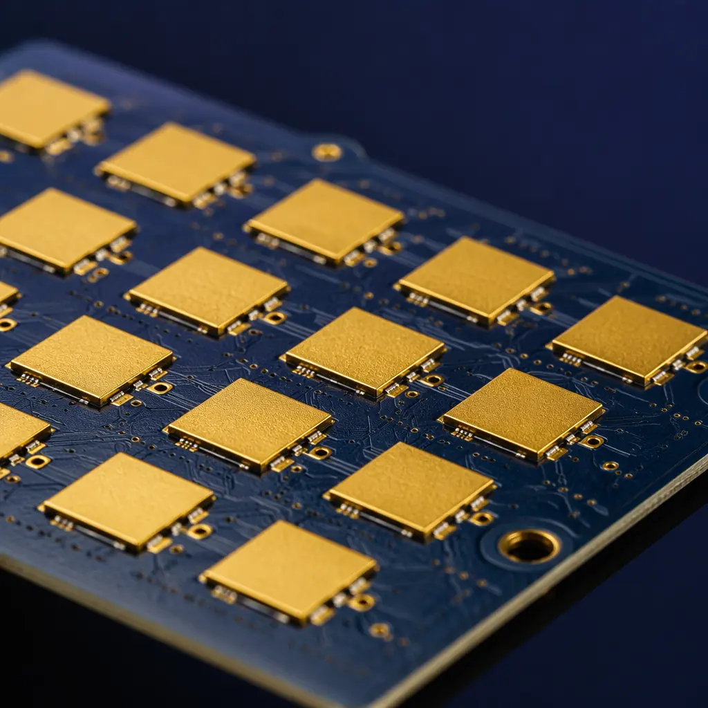
Complete guide to PCB design for 5G mmWave at 28 GHz and 39 GHz. Covers low-loss laminate selection, antenna integration, launch design, and fabrication toleran
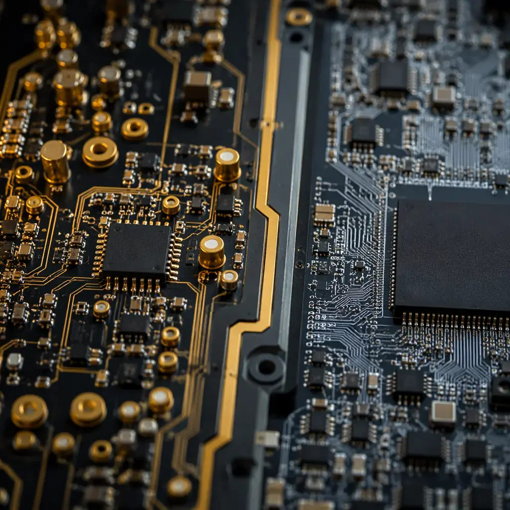
Mixed-signal PCB design guide: analog-digital partitioning, ground plane strategies, isolation techniques, and layer stackup optimization — with production data
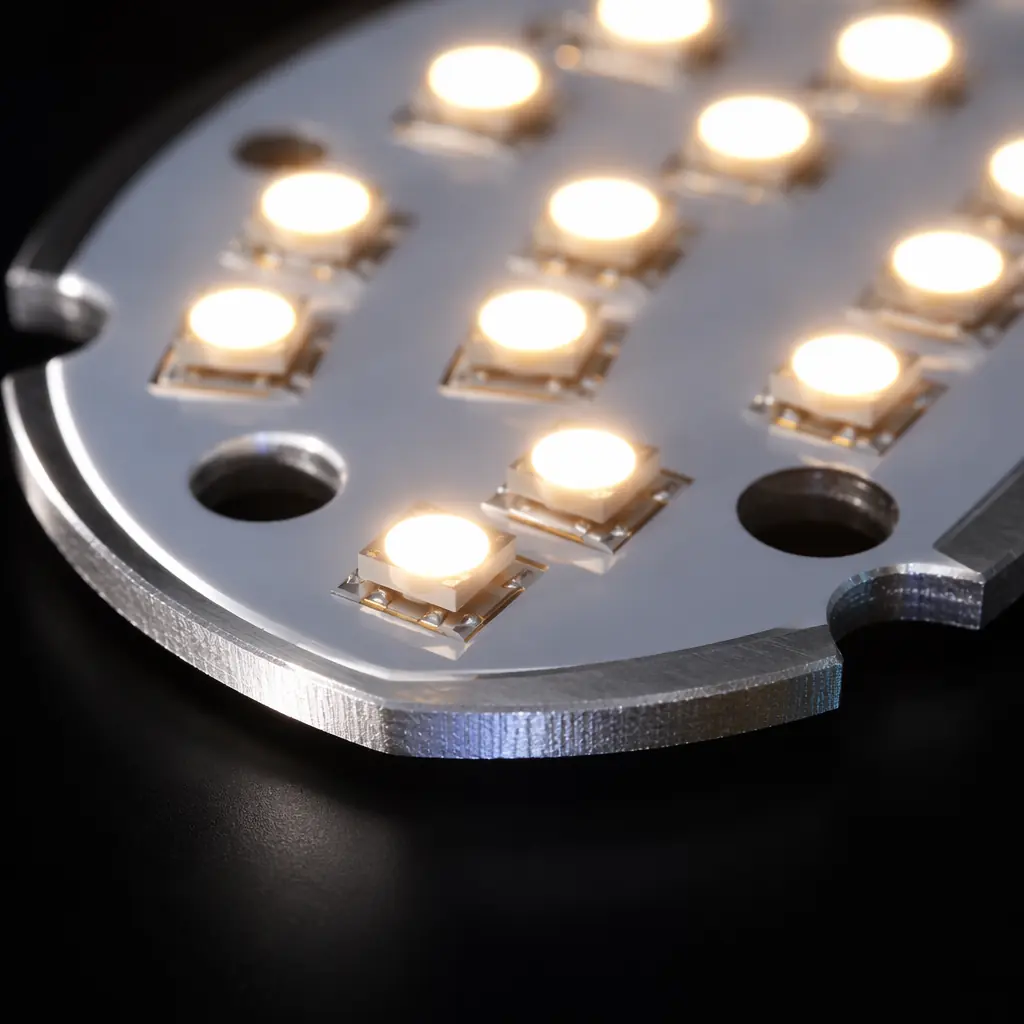
Complete guide to metal core PCB (MCPCB) manufacturing: aluminum vs copper core selection, thermal conductivity benchmarks (1-8 W/m·K), Bergquist and Laird diel
Upload your Gerber files and BOM. We'll respond within 24 hours with a detailed quote and free DFM review.