

Blog
Technical articles on PCB design, manufacturing, and industry best practices. Written by our engineering team.
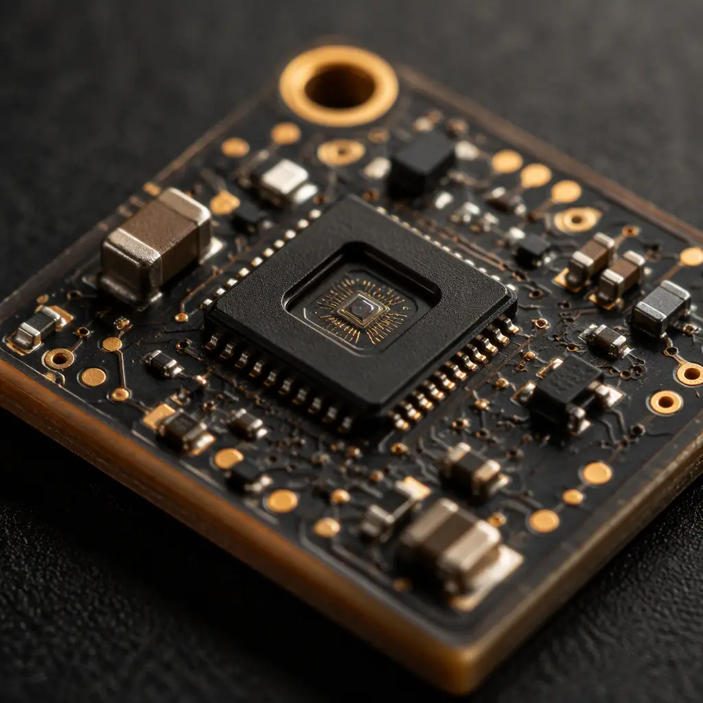
MEMS sensor PCB design rules — accelerometer, gyroscope and pressure sensor layout, analog grounding, package selection, reflow and assembly practices that prot
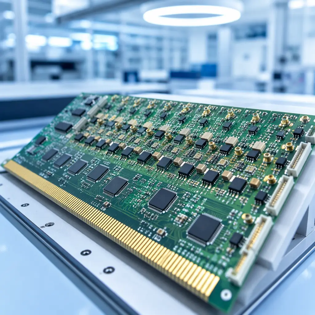
PCB design and manufacturing guide for medical diagnostic and imaging equipment. Covers CT scanner detector boards, MRI gradient amplifier PCBs, ultrasound tran
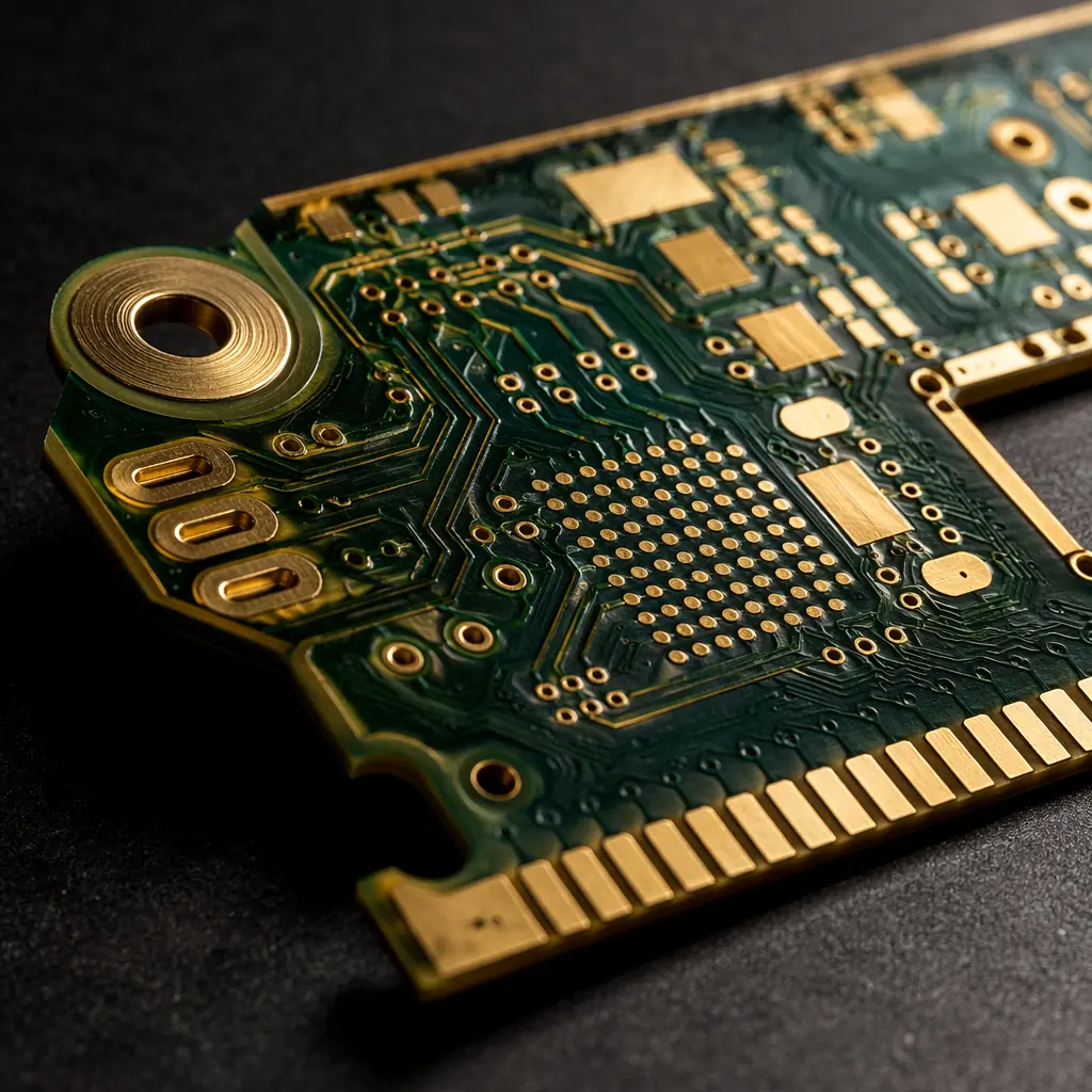
Complete guide to medical device PCB requirements: IPC Class 3 manufacturing, ISO 13485 documentation, biocompatible materials, sterilization compatibility, and
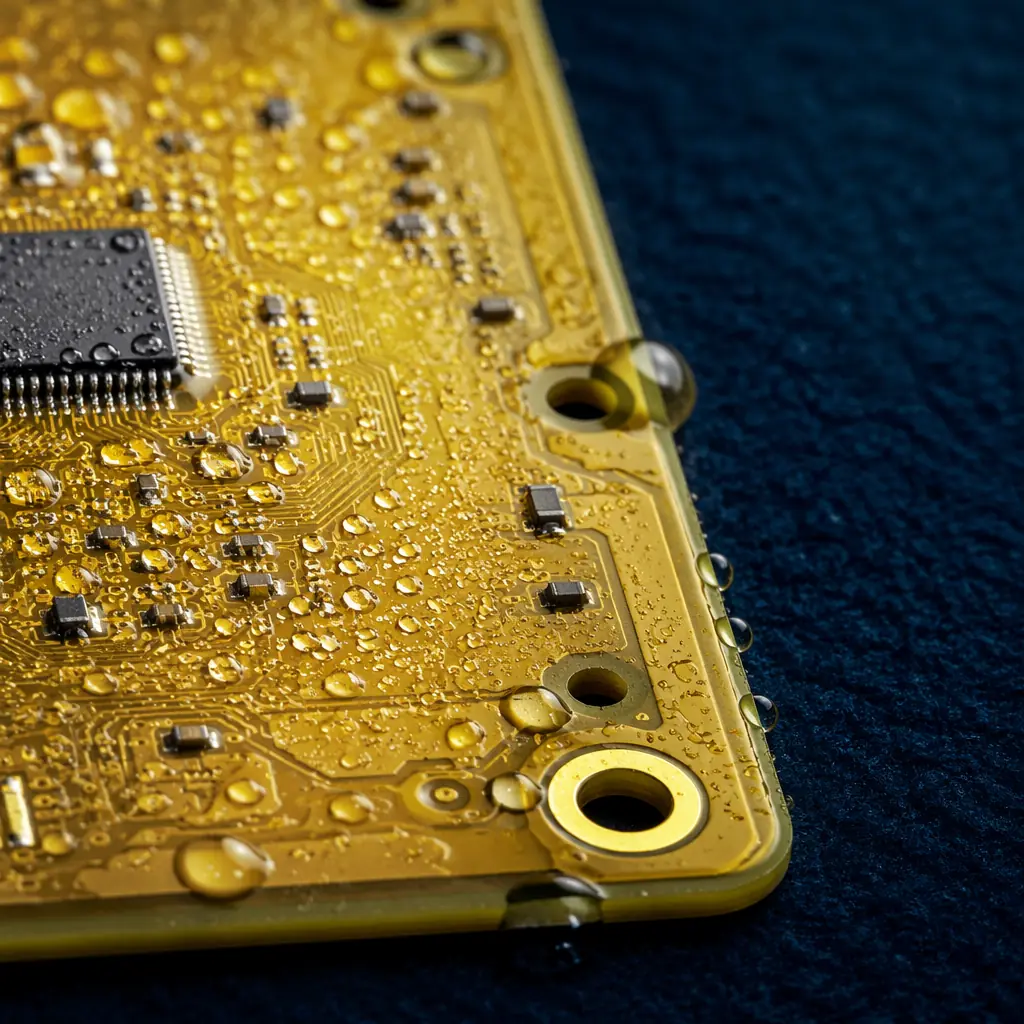
Marine-grade PCB manufacturing for saltwater and offshore environments. Covers salt spray corrosion mechanisms, material selection (laminates/surface finishes),
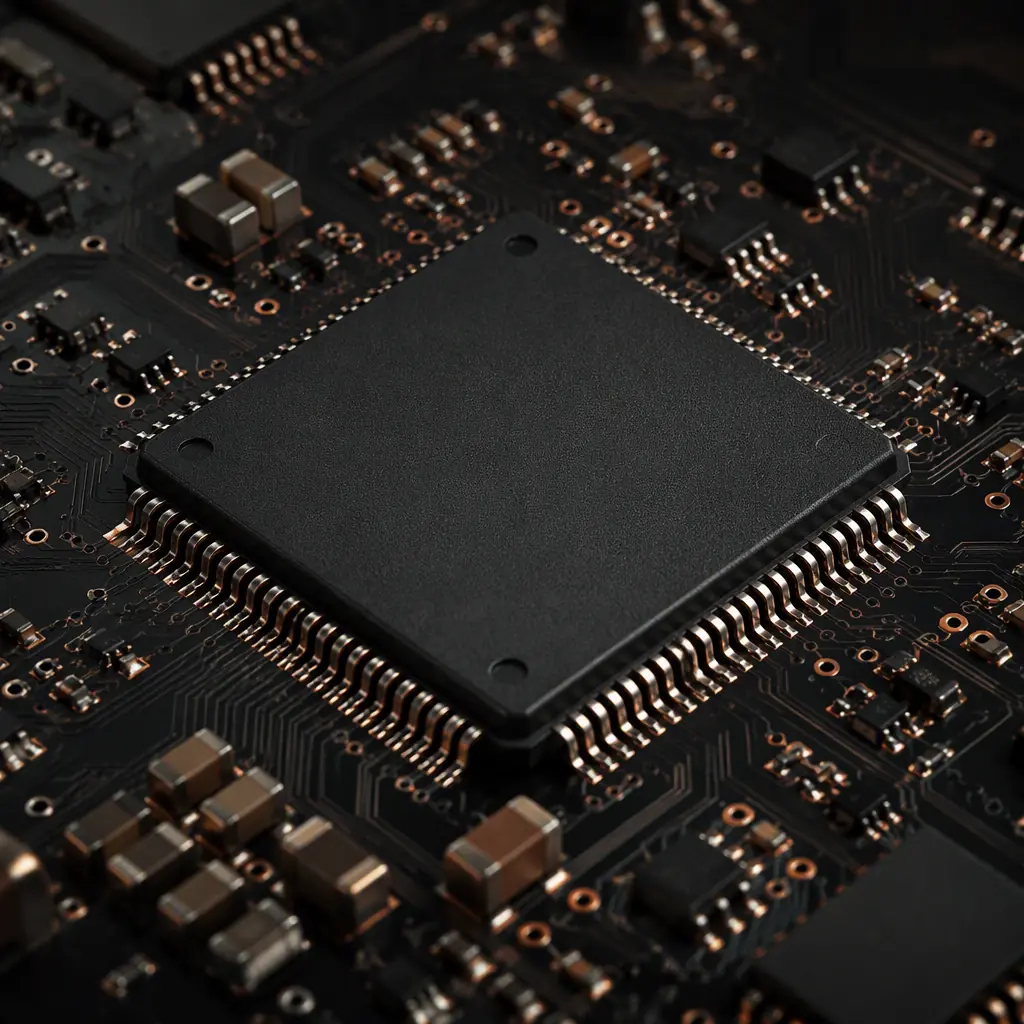
MCU PCB design guide — power decoupling placement, crystal oscillator layout and load capacitors, analog grounding for ADC accuracy, SWD debug port design, and
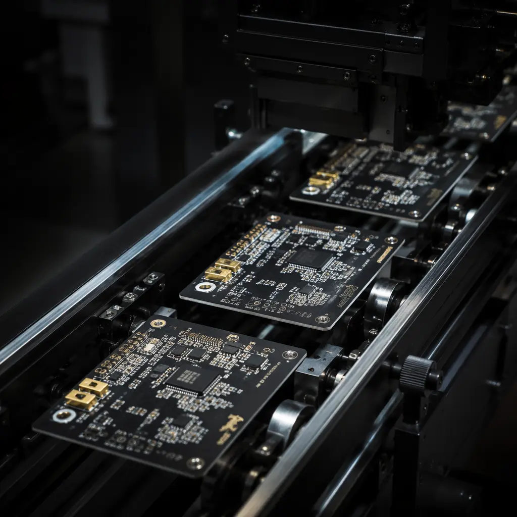
Low-volume PCB assembly for 50-500 units without MOQ penalties. Covers NRE cost reduction, panel sharing, negotiation tactics, minimum order value vs MOQ, and q

LoRaWAN and sub-GHz PCB design guide — 868/915 MHz RF front-end layout, antenna options and matching network, battery-life engineering for LPWAN sensors, certif
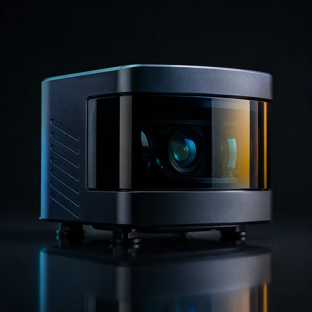
LiDAR PCB design guide: SPAD photodetector arrays, VCSEL laser drivers, high-speed point-cloud data paths and thermal management for automotive and robotics sen
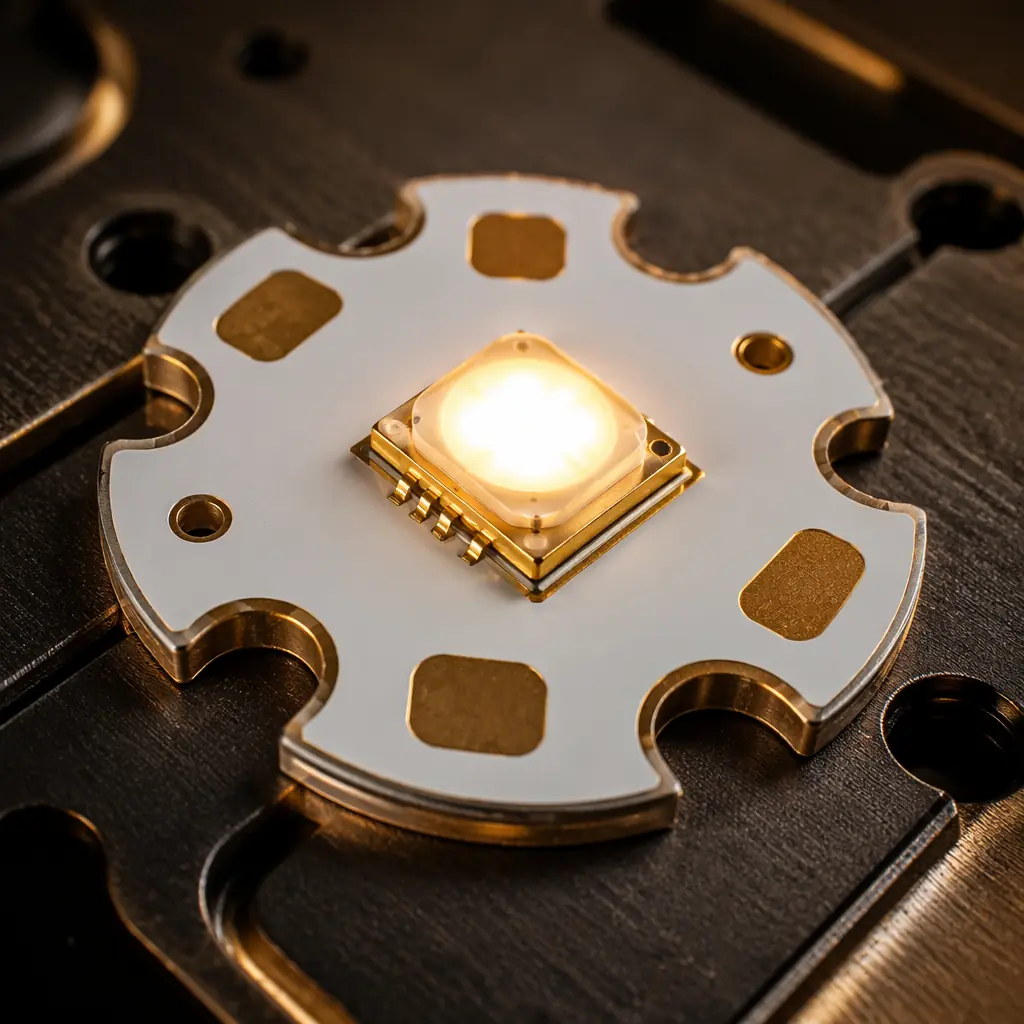
Complete guide to LED PCB manufacturing: aluminum MCPCB thermal design (1-8 W/m·K dielectric), white solder mask reflectivity benchmarks, SMD vs COB layout trad
Upload your Gerber files and BOM. We'll respond within 24 hours with a detailed quote and free DFM review.