

Blog
Technical articles on PCB design, manufacturing, and industry best practices. Written by our engineering team.
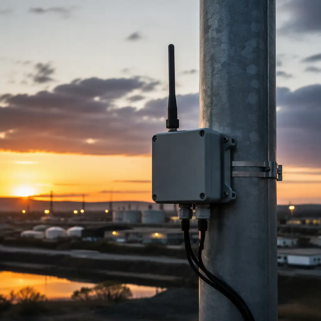
LoRaWAN and sub-GHz PCB design guide covering 868/915 MHz RF front-end layout, antenna options and matching, battery-life engineering for LPWAN sensors
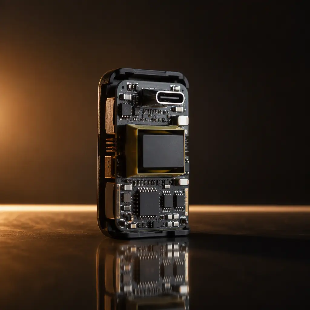
GaN USB-C fast charger PCB design guide covering 65W to 240W power stage layout, loop inductance and gate drive rules, thermal management, EMI control
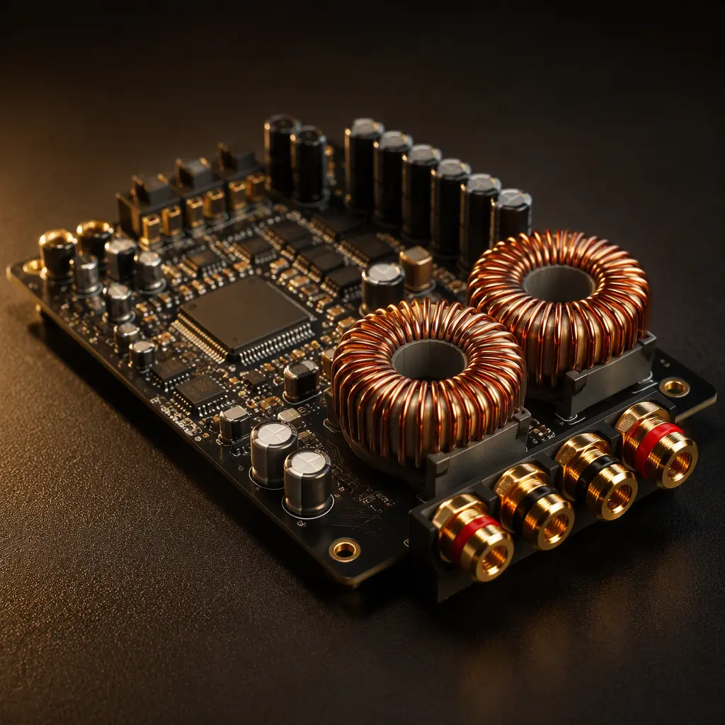
Class-D audio amplifier PCB design guide covering half-bridge power stage, gate drive layout, LC output filter selection and switching-noise control
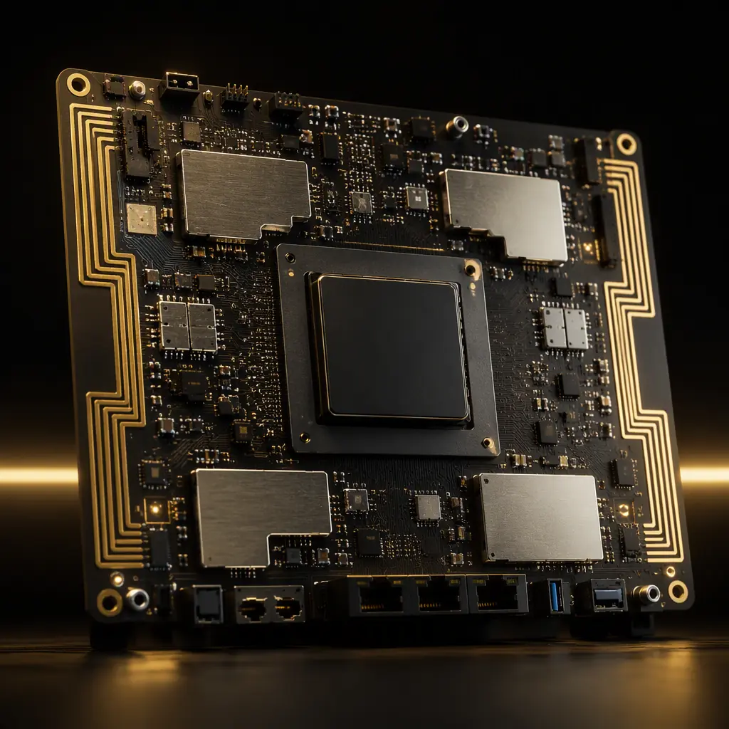
Wi-Fi 7 and Wi-Fi 6E PCB design rules: 6 GHz stackup and material selection, 50 Ω routing with real tolerance, antenna keep-out zones, via stubs

Compare US and Chinese PCB manufacturing for 2026: board costs, lead times, tariffs and landed cost, quality control, IP protection
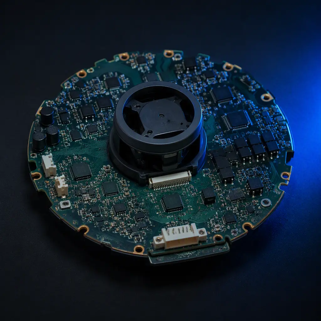
Robot vacuum PCB design and manufacturing guide covering LiDAR/ToF navigation, BLDC motor drive, BMS and charging contacts, mopping-model waterproofing
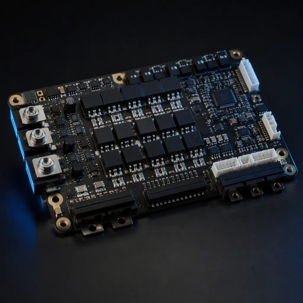
Portable power station PCB design and manufacturing: BMS cell balancing, high-current heavy-copper bus design, sine-wave inverter, MPPT input

PCB payment terms for international buyers and how to protect your payment against quality and fraud risk

AQL sampling for PCB and PCBA inspection: how to read ISO 2859-1 / ANSI Z1.4 tables, choose inspection level and defect classes
Upload your Gerber files and BOM. We'll respond within 24 hours with a detailed quote and free DFM review.