

Blog
Technical articles on PCB design, manufacturing, and industry best practices. Written by our engineering team.
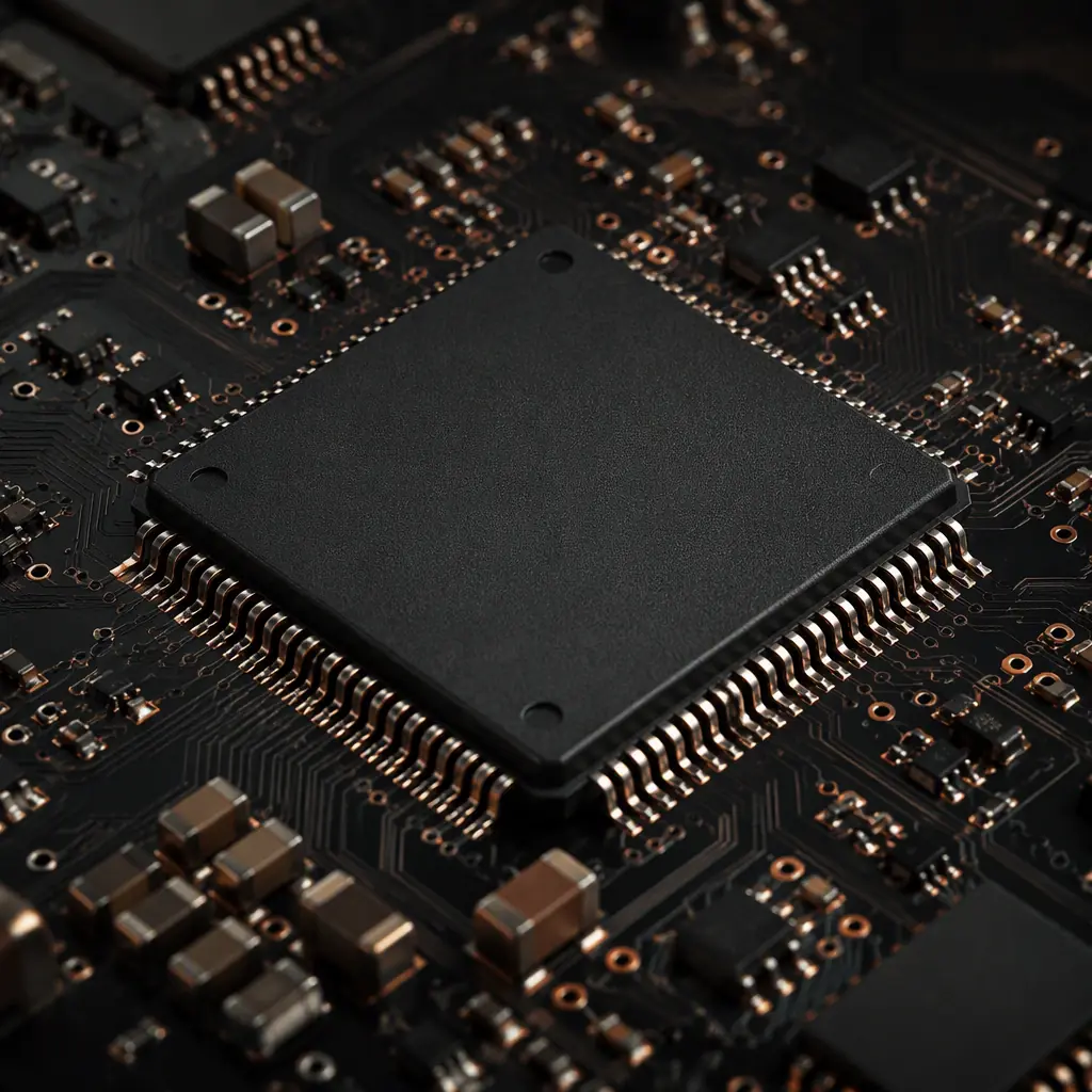
MCU PCB design guide covering power decoupling placement, crystal oscillator layout and load capacitors, analog grounding for ADC accuracy, SWD debug
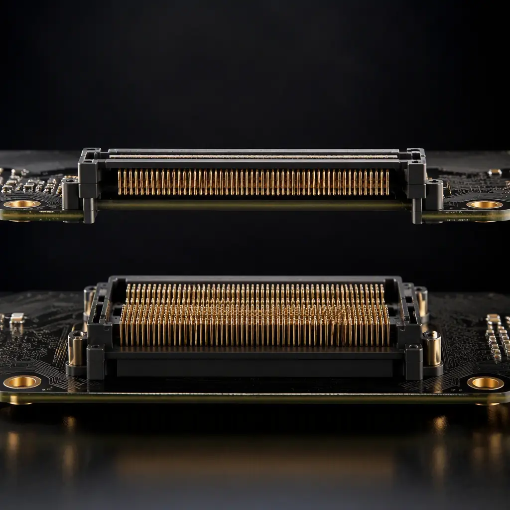
High-speed connector PCB design guide covering board-to-board, mezzanine and backplane connector selection, and differential pair routing through pin fields
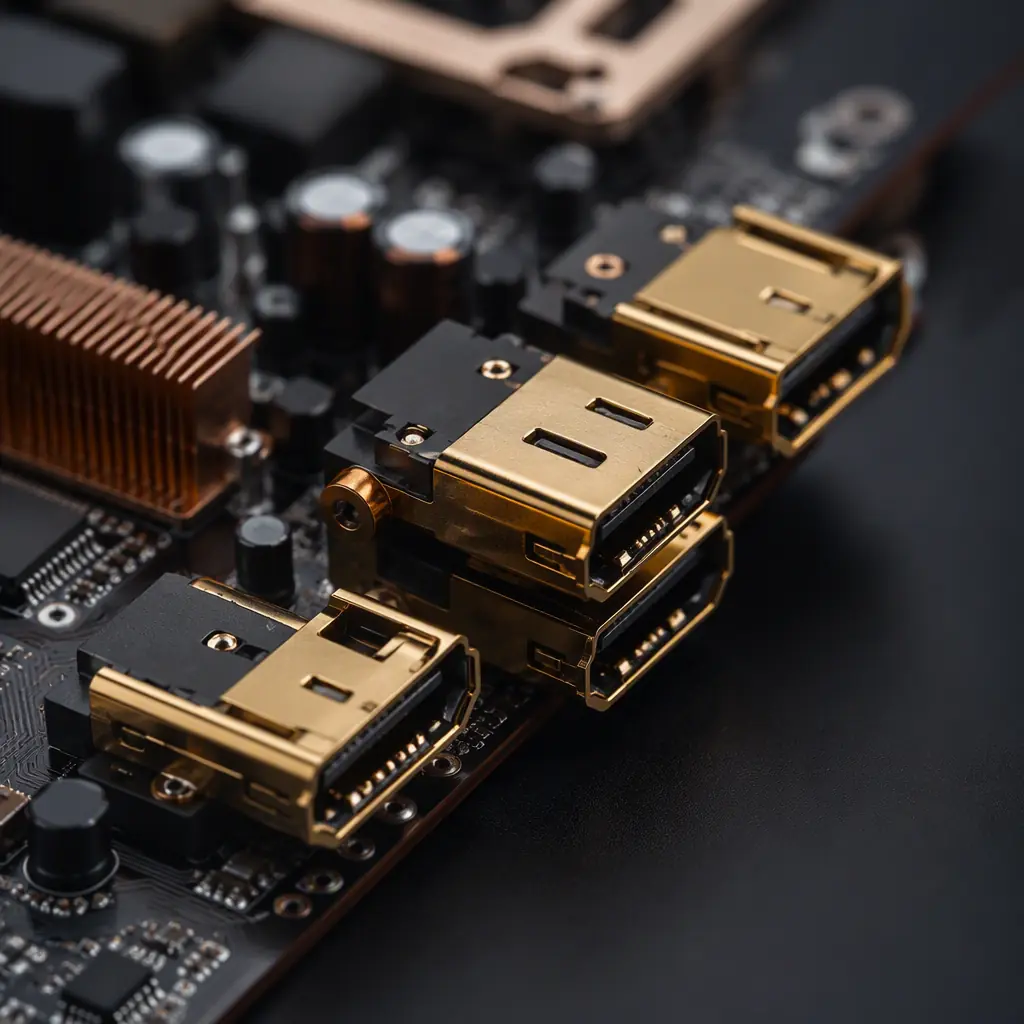
HDMI and DisplayPort PCB design guide covering 100Ω differential pair routing, TMDS vs FRL vs UHBR requirements, ESD protection
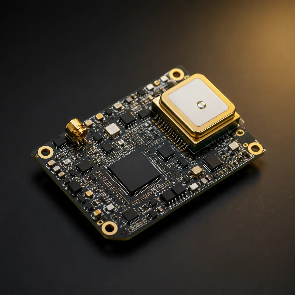
GNSS receiver PCB design rules for GPS, GLONASS, Galileo and BeiDou modules, shielding and assembly checks that determine real positioning accuracy
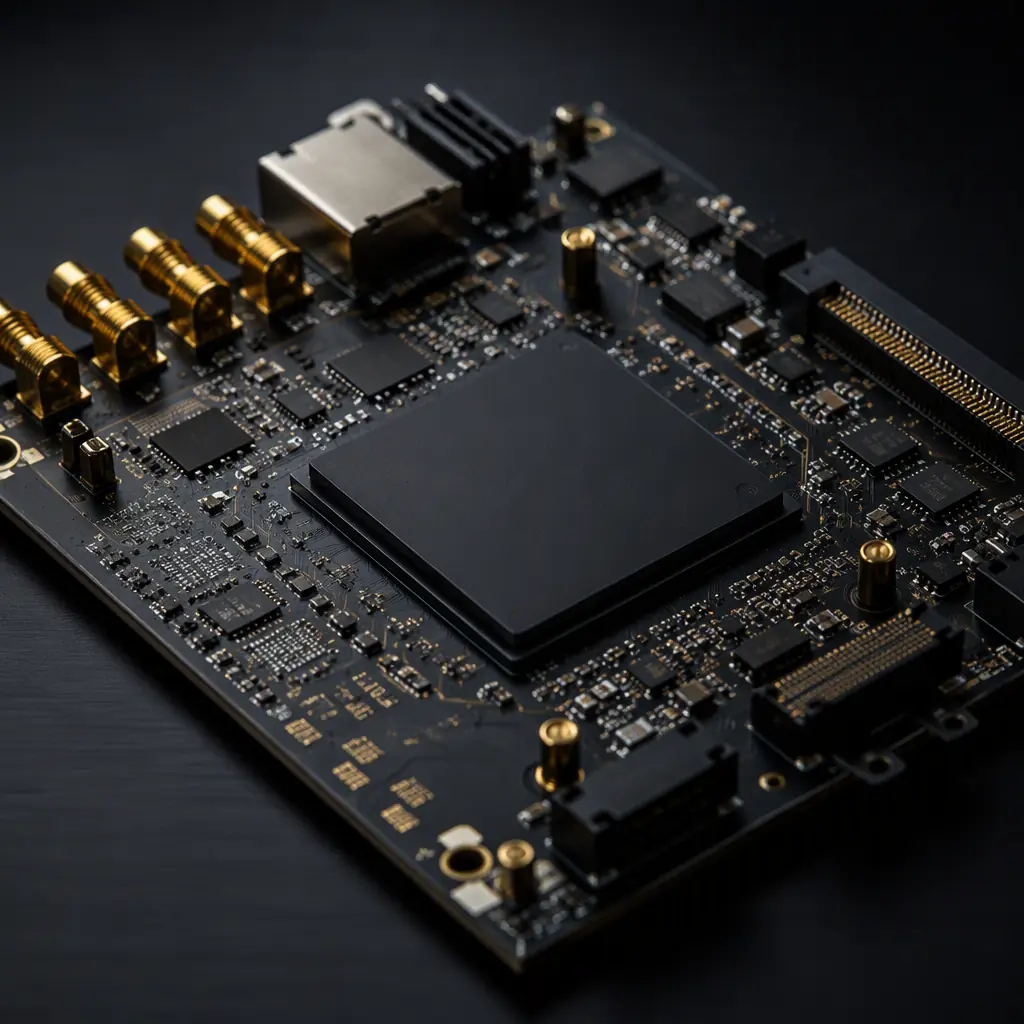
FPGA PCB design rules for Xilinx and Intel FPGAs: power sequencing, decoupling capacitor networks, layer stackup, high-speed I/O routing
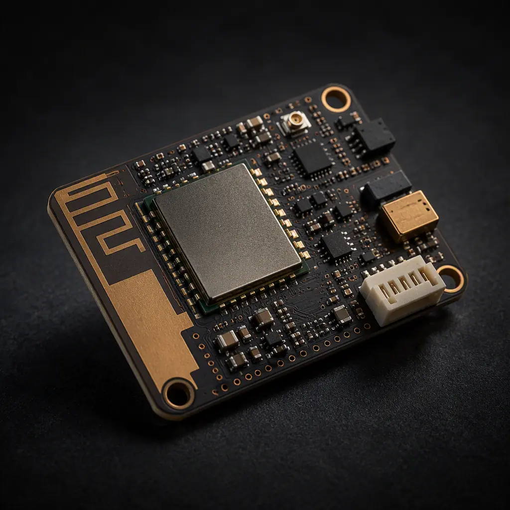
Cellular IoT module PCB design guide covering LTE-M vs NB-IoT vs Cat-1 selection, antenna keep-out, 50 ohm RF trace routing and burst power design
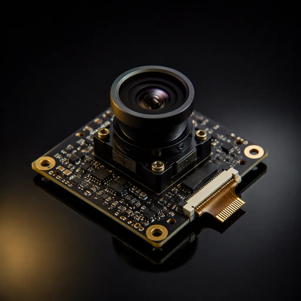
Camera module and image sensor PCB design guide covering MIPI CSI-2 differential pair routing, sensor power supply noise control, clock and EMI management
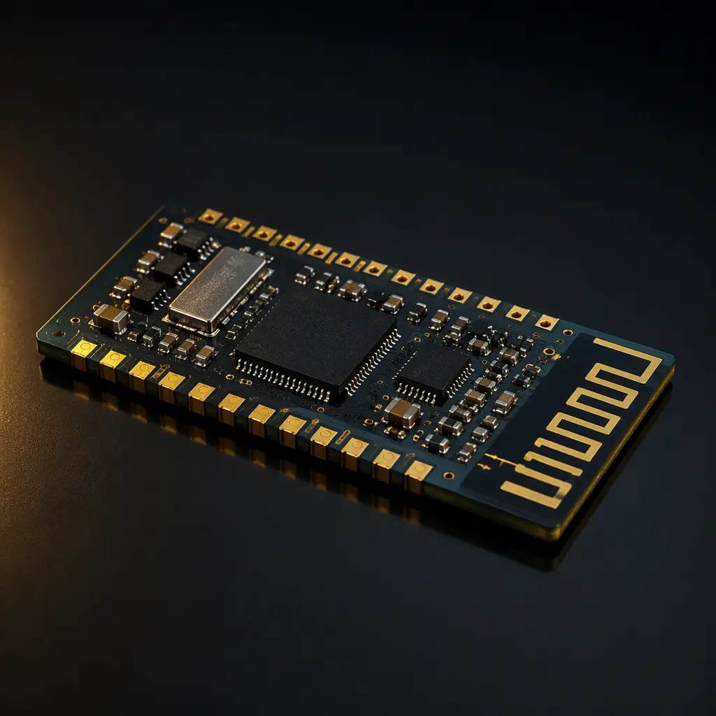
BLE PCB design guide covering 2.4 GHz trace and chip antenna layout, 50 ohm matching networks, crystal and decoupling rules, Wi-Fi coexistence
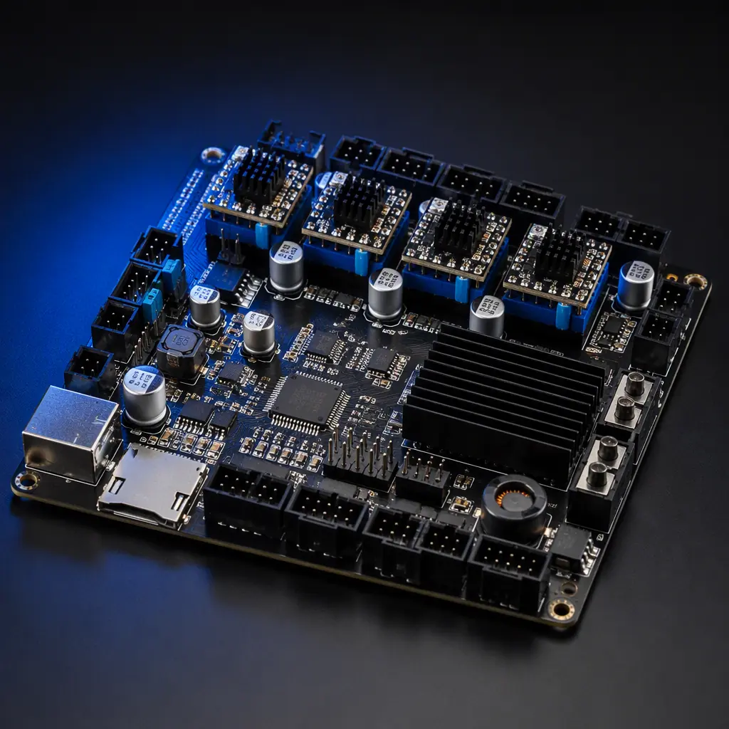
3D printer mainboard PCB design and manufacturing: stepper driver selection, heated-bed MOSFET sizing, thermistor accuracy, 12V vs 24V power architecture
Upload your Gerber files and BOM. We'll respond within 24 hours with a detailed quote and free DFM review.