

Blog
Technical articles on PCB design, manufacturing, and industry best practices. Written by our engineering team.
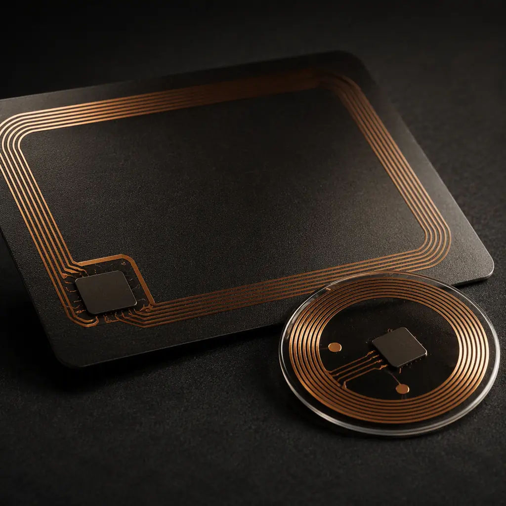
Engineering guide to RFID and NFC antenna PCB design: 13.56MHz coil antenna tuning, UHF 860-960MHz impedance matching, antenna-on-PCB manufacturing tolerances
Complete guide to PCB warpage control: root cause analysis, IPC-TM-650 measurement methodology, design and material strategies
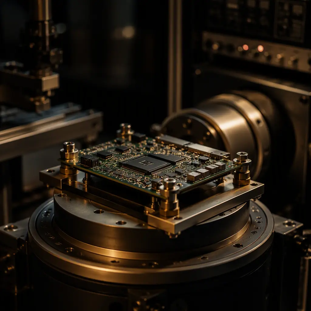
PCB vibration and shock testing guide covering JESD22-B103/B104 and MIL-STD-810 test methods, fixture design, acceleration levels

PCB thermal cycling testing guide covering IPC-9701 and JESD22-A104 methods, temperature ranges, dwell times and Weibull solder fatigue analysis
A step-by-step guide to migrating PCB production to a new supplier: pre-transition audit, phased ramp-up, FAI requirements, overlap management

PPAP for PCB assembly explained. PPAP vs FAI vs ISIR, and the supplier red flags procurement engineers must catch
PCB manufacturing for satellite and LEO constellation electronics: radiation-hardened design, low-outgassing materials, thermal vacuum cycling reliability
How to audit a PCB factory remotely: a step-by-step virtual inspection guide covering video walkthroughs, document verification, process capability checks
Complete guide to PCB press-fit technology, and reliability advantages over soldered connectors for automotive and industrial power electronics
Upload your Gerber files and BOM. We'll respond within 24 hours with a detailed quote and free DFM review.